Case Studies - Banking
Original HTML

Case Studies - Banking

-

Late disclosure of higher mortgage insurance premium leads to added costs for homebuyers and low settlement Mr. and Ms. D wanted to purchase a home and applied for a mortgage. Because their down payment was less than 20% of the purchase price, the mortgage was required to be insured under Canadian mortgage rules, and the bank arranged mortgage insurance as part of the financing.

-

Missing delivery leads to credit card chargeback dispute Mr. D used a credit card issued by Bank A to pay for online purchases from a Chinese e‑commerce platform in June 2025. The seller provided Mr. D with a tracking number shortly after the purchase. However, the tracking information never showed any shipping activity beyond its initial creation. The estimated delivery date passed without the goods being delivered. Mr. D attempted to resolve the issue by contacting the seller through the platform, but the seller did not provide a meaningful response. Mr. D did not receive a refund or a replacement.

-

Missed payments result in increased interest costs for consumer after balance transfer Ms. J held a credit card with her bank for several years when she learned of a promotional offer that allowed customers to transfer balances from other credit cards to her bank’s credit card at a 0% interest rate for 12 months. She called the bank to ask about this offer and the bank confirmed that it was still available, with a 3% balance transfer fee.

-

Consumer challenges interest charges after accepting balance transfer promotion Ms. W was a smart credit card user, always making sure to pay off her balance in full each month. She used her cashback card for everything from travel expenses to groceries, and for cash advances. Her bank informed her of a promotional offer to transfer balances from other credit cards to her cashback card at a 0% interest rate for 12 months. This offer represented a significant savings from the usual interest rates of 20.99% on outstanding balances and 21.99% on cash advances.

-

Consumer a victim of fraud but bank not responsible for loss Mr. E had a personal chequing and savings account at Bank Y. He enjoyed the convenience of online banking on his laptop and cell phone, and often accessed his bank accounts using Bank Y’s mobile application. Through e-mail, he received notifications from the bank about his account activity and liked being able to confirm account balances online. Mr. E had been a Bank Y customer for over 40 years.

-

Bank customer questions significant fees charged to his business account Mr. G had been a loyal business customer of his bank for 30 years. He trusted the bank with his business’ financial matters, and they had always maintained a good relationship.

-

Consumer is not responsible for bank’s technical issues Ms. Q returned to Canada from living abroad. To re-establish her credit history, she applied for and received a prepaid credit card, which held a cash balance and was widely accepted. She used this card to pay bills and make online purchases, such as groceries. The mobile app associated with Ms. Q’s prepaid credit card allowed her to easily add funds to her account, monitor her spending and review her monthly account statements online.

-

Consumer surprised when bank gives him 30 days to close his account Mr. K arranged a meeting at a Canadian branch of ABC Bank, so he could open a personal chequing account. At the meeting, he provided the proper documentation and told the bank he would be traveling abroad. He also mentioned that a branch of ABC Bank was located where he was going, and he was relying on his new ABC bank account to transfer money back to Canada.

-

Consumer pursues credit card refund for vacation cancelled due to COVID-19 Whenever you buy goods and services, especially for future delivery, be sure to pay careful attention to the terms and conditions of the purchase. Return and refund policies vary, so before you agree to buy, it’s important to understand what you will be entitled to if the goods are damaged, or the services are cancelled.

-

Consumer responsible for unauthorized transactions after not taking enough care to protect his debit card and PIN If you have a debit card, you have agreed to use it subject to the obligations in the cardholder agreement you made with your bank when the card was issued.

Class (B2B/B2C)
B2C
Ingest Status
Rewritten
Dedupe hash
7c7fc123aaf383b51d54ac1470414629
Press Eligible
Yes
Press Eligible Reason
Manuelle Prüfung nötig. Risiko: MEDIUM. Flags: ['finance', 'numbers']. Stichprobe: True
Source Name
Ombudsman for Banking Services and Investments (OBSI)
Image URL
https://media-001-ca.cdn.govstack.com/obsi-006-ca/media/1byowuih/obsi-logo-cropped.svg
Content Hash (SHA-256, erste 32 hex)
6f51523a7f77faaafcd2be8f20a2c8ec
Yeti Audio-Animatronic Coming Back to Life Inside Expedition Everest
Image File
Original HTML

On the “Horizons: A Carousel of Progress” stage at D23: The Ultimate Disney Fan Event presented by Visa, Neil Patrick Harris was interrupted by Thomas Mazloum, Chairman, Disney Experiences. It was time for an announcement big enough to shake a mountain to its core: “We’re bringing the Yeti back to life inside Expedition Everest at Disney’s Animal Kingdom!”

Cheers rocked the crowd, louder than the screech of a legendary beast.

As beasts of legend are soothed with song, Gloria Gaynor gave our long-dancing yeti an epic send-off. She paid tribute to our loveable Yeti as only she could, performing her 1978 disco hit, I Will Survive.

Expedition Everest at Animal Kingdom

Nestled inside Disney’s Animal Kingdom, a majestic (and nearly 200-foot) Forbidden Mountain houses a legendary secret. From the moment you enter the queue, the lore of the yeti comes alive, as you peruse a trailside museum featuring evidence of campground attacks, sketches of sightings, and even a footprint mold of a giant yeti foot.

Once you’ve boarded an old tea train car and climbed the rocky peaks, you’ll notice a few more obvious signs of the mysterious guardian of the mountain during the high-speed ride, including a few torn train tracks. Inspired by the northwest face of Mount Everest and geological elements found in Tibet and Nepal, Expedition Everest is the perfect hideout for even the most discerning yeti.

Stay tuned to Disney Parks Blog. We’ll have all the latest news on this star of the Himalayas.

Class (B2B/B2C)
B2C
Ingest Status
Rewritten
Dedupe hash
aa1802e39a9b2e06d6323c104b3eac12
Press Eligible
Yes
Press Eligible Reason
Disney announces an update to a theme-park attraction for visitors.
Source Name
Disney Parks Blog
Image URL
https://disneyparksblog.com/app/uploads/2026/08/YETI-Animal-Kingdom.png
Source Node
Content Hash (SHA-256, erste 32 hex)
e14c59eca07b287141cc6134c0d19a96
A Grand and Miraculous Refurbishment: Spaceship Earth to Receive Reimagining
Image File
Original HTML

We now know the future of Spaceship Earth at EPCOT.

As Neil Patrick Harris was talking about outer space on the Horizons: A Carousel of Progress stage at D23: The Ultimate Disney Fan Event presented by Visa, conversation naturally shifted to our favorite geodesic sphere from the ‘80s.

Makes sense. How can you talk about the future of Disney Experiences without discussing the iconic attraction that celebrates humanity’s march from the caves to the cosmos and inspires guests to imagine, create, and build a better tomorrow.

Joining him onstage to talk about the engineering marvel were Disney Imagineer Ali Rubinstein and YouTuber Mark Rober. This dynamic duo gave a nice refresher on the iconic opening day EPCOT attraction before jumping into the anticipated news.

For the first time in nearly 20 years, Spaceship Earth is getting an update.

The Evolution of Spaceship Earth

Before our ride vehicle turns around and takes us into the future, let’s celebrate the legacy of Spaceship Earth, a groundbreaking attraction that has inspired guests for generations.

Fun Facts about Spaceship Earth

- Walter Cronkite narrated a script that was added to the attraction in 1986. In fact, since opening, there have been four narrators for Spaceship Earth.

- The structure is called a “geodesic sphere” because it’s a perfectly round structure that is supported in the air by three pillars.

- The attraction stands at 180 feet tall with 2.2 million cubic square feet of space inside the geosphere.

- Spaceship Earth is one of the most complicated ride systems Walt Disney Imagineering has ever created because the ride incorporates a continuously moving train of vehicles that spiral up into the structure before turning “backward” to come back down to Earth.

- The storyline currently follows the history of human innovation, from prehistoric times to the 21st century.

Like the attraction, the evolution of Spaceship Earth has been an exciting journey filled with chapters of progress, displays of ingenuity, and an endless future of invention.

Updates Coming to Spaceship Earth

It’s time to invent the future! At the showcase, Ali revealed that a re-imagineered Spaceship Earth will be coming to EPCOT, bringing the attraction into the internet age and beyond.

What can you expect in the world of tomorrow? The ride currently tells the story of human communication, but the team is reimagining that focus on a broader theme that is still classically EPCOT – human connection.

So, here’s to the next 30,000 years on Spaceship Earth. The present is just the beginning!

Class (B2B/B2C)
B2C
Ingest Status
Rewritten
Dedupe hash
dc71df375625845d1019873adbe964ab
Press Eligible
Yes
Press Eligible Reason
Disney announces a consumer-facing update to the Spaceship Earth attraction at EPCOT.
Source Name
Disney Parks Blog
Image URL
https://disneyparksblog.com/app/uploads/2026/08/DSC6335-scaled.jpg
Source Node
Content Hash (SHA-256, erste 32 hex)
6e47597f605e3649411c5490527df504
Dreamfinder and Figment Return to EPCOT
Image File
Original HTML

There’s one more surprise coming out of Horizons: A Carousel of Progress. And it’s the only thing host Neil Patrick Harris asked for! Aside from unlimited churros during the event.

Ok, picture this: two tiny wings, eyes big and yellow. The horns of a steer (but don’t worry, he’s a lovable fellow). From head to tail, he’s a royal purple pigment. Are you imagining it? Good, because voila — you’ve got a Figment!

Announced during the closing moments of the Disney Experiences showcase at D23: The Ultimate Disney Fan Event presented by Visa, it’s time to take a new flight of fancy into our imagination at EPCOT. Not only will everyone’s favorite creative purple dragon be sticking around, but he’s finally reunited with Dreamfinder, too.

You know what they say: a dream can be a dream come true.

“We are taking a new journey into imagination at EPCOT with Dreamfinder and Figment!” Disney Experiences Chairman Thomas Mazloum told the cheering crowd. “I’m so happy to share this news tonight. We know how important this is to you. We’ve heard you, and this is one more way we’re putting you in the center of everything we do.”

There’s so much more to come about Dreamfinder and Figment’s journey back to EPCOT, but it’s not like either one of them has totally disappeared from our hearts.

Who is Figment?

Unless you’ve been living under a geodesic sphere for the last few years, you’ve probably seen Figment out and about around EPCOT — both doing meet-and-greets in the Imagination! pavilion, and adorning copious amounts of EPCOT and festival merchandise. Figment has been the focal point for EPCOT International Festival of the Arts since the inaugural season back in 2017. His most recent resurgence kicked off with a viral novelty popcorn bucket in 2022.

But Figment’s been at EPCOT since 1983 when the first iteration of Journey into Imagination opened. While the attraction has been through a few different versions over the years, that loveable purple dragon has always been a staple in the park, becoming one of the park’s most recognizable and enduring icons.

As the embodiment of imagination itself, part of what makes Figment so special is that he’s uniquely EPCOT. His curiosity and playfulness most represent the identity of EPCOT as a park.

Who is Dreamfinder?

Before there was Figment, there was Dreamfinder, the whimsical dream-chaser who helped bring imagination to life. Introduced in the original Journey Into Imagination attraction at EPCOT in 1983, Dreamfinder guided guests “collecting sounds, colors, ideas, anything that sparks the imagination.”

The cheerful inventor and storyteller served as both creator, mentor and friend to Figment, encouraging guests to remain curious. All it takes is one little spark.

For 15 years, from 1983 to 1998, Dreamfinder was at the center of Journey into Imagination, inspiring generations of EPCOT fans with his boundless optimism and sense of wonder. Decades later, fans still hold Dreamfinder close to their hearts, not just because of the adventures he shared with Figment, but because of the feeling he inspired: that imagination is something worth holding onto, no matter how old you are.

Class (B2B/B2C)
B2C
Ingest Status
Rewritten
Dedupe hash
945074ee1095b752724d5fa768db23cb
Press Eligible
Yes
Press Eligible Reason
Manuelle Prüfung nötig. Risiko: LOW. Flags: ['none']. Stichprobe: True
Source Name
Disney Parks Blog
Image URL
https://disneyparksblog.com/app/uploads/2026/08/Figment-and-Dreamfinder.jpg
Source Node
Content Hash (SHA-256, erste 32 hex)
2916217fb75258bd6415964ec04254c6
Quantum Weekly News – your one-stop newsletter for the latest breakthroughs and industry updates in Quantum Computing
Image File
Original HTML

Quantum Weekly News – your one-stop newsletter for the latest breakthroughs and industry updates in Quantum Computing

Global roundup of quantum computing news, research, and policy

This week, the quantum computing world witnessed a mix of global collaboration, technological innovation, and strategic investments that continue to accelerate progress toward large-scale quantum advantage. From new partnerships in Japan to breakthroughs in quantum-secure communications, here’s everything you need to know from the past week.

Government & Institutional Initiatives

🇯🇵 September 29, 2025 | Tokyo, Japan Fujitsu and AIST Announce Strategic Quantum Partnership Fujitsu Ltd. and Japan’s National Institute of Advanced Industrial Science and Technology (AIST) announced a groundbreaking collaboration to advance superconducting quantum computers. The partnership will focus on developing large-scale systems, optimizing cryogenic control electronics, and accelerating commercialization through joint R&D and shared infrastructure. 🔗 Source: Fujitsu Global Press Release

Industry Developments

🇺🇸 September 29, 2025 | Denver, Colorado Quantum Computing Inc. (QCi) Unveils Quantum-Secure Communication Platform At the ECOC 2025 Conference, Quantum Computing Inc. demonstrated its “Quantum Secure Solution,” a high-dimensional time-energy entangled communication platform. The system is designed for integration with existing telecom networks, offering a scalable pathway toward quantum-safe data transmission for commercial and defense sectors. 🔗 Source: Quantum Computing Inc. Press Release

🇩🇪 September 30, 2025 | Garching, Germany Kiutra Secures €13 Million in Series A Funding Kiutra, a startup specializing in cryogenic cooling systems for quantum computers, successfully closed a €13 million funding round. The company’s innovation — cooling without helium-3 — addresses one of the most critical bottlenecks in scaling quantum hardware. 🔗 Source: Company Announcement, Garching Tech Week 2025

Research & Academic Highlights

🇺🇸 September 29, 2025 | Cambridge, Massachusetts Harvard Researchers Control 3,000+ Qubit System A team at Harvard University reported controlling over 3,000 neutral atom qubits, marking one of the largest experimental quantum systems to date. The breakthrough, published in Physical Review Letters, demonstrates long-coherence control and advances the pursuit of fault-tolerant quantum architectures. 🔗 Source: Harvard Quantum Initiative Journal Publication

October 1, 2025 | Leuven, Belgium & Sydney, Australia Diraq and imec Achieve Scalable Silicon Quantum Dot Fabrication Australian quantum firm Diraq, in collaboration with Belgium’s imec, announced a major advance in silicon quantum dot manufacturing. Their results, achieved using standard CMOS fabrication techniques, bring the industry closer to mass-producible quantum chips. 🔗 Source: imec Global Newsroom

Recommended by LinkedIn

Education & Talent Development

🇺🇸 October 2, 2025 | Albuquerque, New Mexico Launch of the Quantum Learning Lab (QuLL) The Quantum Learning Lab officially opened this week, offering hands-on training programs for engineers, scientists, and students entering the quantum field. The lab’s first “Quantum Technician Bootcamp” began on September 29, emphasizing applied skills for hardware calibration and quantum error mitigation. 🔗 Source: New Mexico Tech Innovation Press Brief

Conferences & Forthcoming Events

🇮🇱 October 3, 2025 | Tel Aviv, Israel Quantum Machines Announces AQC25 Conference Quantum Machines unveiled the Adaptive Quantum Circuits 2025 (AQC25) conference, to be held in November. The event will convene global researchers and industry leaders to discuss adaptive mid-circuit quantum algorithms — a key frontier for real-time feedback and fault tolerance. 🔗 Source: PR Newswire

Awards & Recognitions

🇸🇪 October 3, 2025 | Stockholm, Sweden Nobel Prize in Physics 2025 Awarded for Quantum Circuit Experiments The 2025 Nobel Prize in Physics was awarded to three scientists whose pioneering experiments demonstrated quantum effects in macroscopic electrical circuits — the foundation for superconducting quantum computers. This recognition highlights how fundamental physics continues to shape modern technology. 🔗 Source: Royal Swedish Academy of Sciences Press Release

Global Policy & Outlook

🇺🇸 October 5, 2025 | Washington, D.C. White House OSTP Reaffirms Quantum as National Priority The U.S. Office of Science and Technology Policy emphasized continued quantum R&D investment as part of its fiscal 2026 science priorities. The initiative focuses on quantum-safe cryptography, scalable architectures, and quantum networking infrastructure. 🔗 Source: OSTP Blog Post — “Science Priorities for the Next Frontier”

Summary: The Quantum Frontier Is Accelerating

From Japan’s national partnership and Harvard’s record qubit control, to multi-million-dollar investments and policy-level reaffirmations, this week has underlined one thing: quantum computing is no longer experimental — it’s infrastructural. Momentum is global, collaboration is key, and the line between research and commercialization is rapidly disappearing.

Thanks for sharing

𝗦𝘂𝗯𝘀𝗰𝗿𝗶𝗯𝗲 𝘁𝗼 𝗺𝘆 𝗬𝗼𝘂𝗧𝘂𝗯𝗲 𝗰𝗵𝗮𝗻𝗻𝗲𝗹 for the latest 𝗾𝘂𝗮𝗻𝘁𝘂𝗺 𝗰𝗮𝗿𝗲𝗲𝗿 𝘂𝗽𝗱𝗮𝘁𝗲𝘀, expert sessions, and research insights from around the world. Youtube Channel link: https://lnkd.in/g8fu8CEk

Class (B2B/B2C)
B2B
Ingest Status
Rewritten
Dedupe hash
acef5514792a913295e42aaa99c708ae
Press Eligible
Yes
Press Eligible Reason
Manuelle Prüfung nötig. Risiko: MEDIUM. Flags: ['finance', 'numbers']. Stichprobe: False
Source Name
GlobalFoundries Newsroom
Image URL
https://media.licdn.com/dms/image/v2/D5612AQFO4Q3-fhB7PQ/article-cover_image-shrink_600_2000/B56ZnUtXsWI4AQ-/0/1760210290984?e=2147483647&v=beta&t=mHYqtgQb4T7JqN1zcvCaZCU_yBJvZC9IIAM6qfBLGos
Content Hash (SHA-256, erste 32 hex)
59cb464d16d774c4d4690fa17dfa43fe
How to Evaluate Quantum Processor’s Performance: In Conversation With Himadri Majumdar*
Image File
Original HTML

How to Evaluate Quantum Processor’s Performance: In Conversation With Himadri Majumdar*

Not all quantum processors are created equal. While everyone aims to increase the fidelity of quantum states and lower the error rate, many other metrics also play an important role in building large-scale quantum computers and delivering commercial value.

SemiQon builds quantum processors by trapping electrons or holes within silicon and using their spins as qubits, called silicon spin qubits. Since its founding as a spinout from the Finnish research institute VTT in 2023 and our last interview on Future of Computing, SemiQon has successfully completed several fab runs and started shipping the first 4-qubit chips to research collaborators.

This article is part of a series of deep dives into SemiQon’s advancements, and we had the pleasure of speaking again with Himadri Majumdar, CEO and co-founder of SemiQon, about what quantum hardware manufacturers and end users should keep in mind when evaluating quantum processors:

What’s the Fidelity of Quantum States?

Fidelity is sort of the counterpart to the error rate, measuring how accurately a quantum state has been prepared, transformed, or measured. It quantifies how close two quantum states are, which is typically the ideal target state and the actual quantum state produced by a quantum operation in the physical world. If you’re familiar with machine learning, think vector similarity but for quantum states.

Fidelity is a critical metric for evaluating the reliability and accuracy of quantum computations. It’s used to demonstrate the capabilities of quantum processors, where achieving high fidelity is often regarded as the holy grail of quantum computing—or simply put, the higher the fidelity, the closer we’re to practically useful quantum computing.

But practically, the important question is: How do we measure fidelity at scale when we have thousands, or eventually millions, of connected qubits? Individual qubits are not very useful unless they’re networked together, which opens up many more questions around: How will the networking be implemented? How will we control and calibrate them individually? And how will the control electronics behave, and what latency will it introduce?

Fidelity is important, but we need to start speaking about fidelity at scale, with connected qubits. We need to consider quantum processors as a whole and look at holistic metrics—this will decide who will build large-scale, useful quantum computers.

What Other Metrics Are Important When Evaluating a Quantum Processor’s Performance?

Quantum hardware manufacturers focus a lot on what their machines are fundamentally capable of: What set of quantum computing operations, called quantum gates, can we implement? What’s our error rate? How often do we need to do error correction?

Most metrics today focus on single qubits or a few qubits, as quantum computers are still rather small. It still takes an unbelievable amount of time to measure and calibrate or tune qubits, which is possible for small qubit numbers but not at scale. We’ll need to evolve our measurement and calibration protocols for scaling. And we need measures that are industrially relevant and doable. So, besides fidelity at scale, there are various other metrics one should keep in mind, such as the ones that have been proposed in the literature:

Computation speed: to compensate for low coherence time, gate operations should occur fast enough to make complex computations

Multiqubit networking: the more qubits can be linked to one another to perform gate operations, the more readily they can implement quantum computing algorithms and the more powerful the resulting quantum computer would be

Control over individual qubits at scale: as the number of qubits in a quantum computing system increases, control over the performance of individual qubits becomes increasingly complex

Cooling and environmental control: for most qubit technologies, the required cooling equipment needs to scale in terms of both size and power 

Manufacturing: some qubit designs use existing production technology, while others require new manufacturing techniques. The production of full-scale quantum computers will eventually require automated manufacturing and testing for components

The quantum computing industry creates and adapts metrics as it develops further. For example, IBM introduced quantum volume as a metric to measure the computational power of a quantum processor, considering the largest random quantum circuit involving an equal number of qubits and operations that a quantum computer can successfully run.

Rather than just considering the number of qubits, it also accounts for other factors such as their interconnectedness, error rates, and coherence times. But it doesn’t describe computational power across multiple quantum chips well. As manufacturers like IBM hit the ceiling on how many superconducting qubits they can pack in a single chip with a reasonably sized dilution refrigerator, they need to develop new metrics that are a better fit for multicore quantum computers and distributed across many dilution refrigerators.

Having all of these metrics can confuse end-users, the buyers of quantum computers or cloud users, as they only care about what solves their industry problems in a commercially viable way. That’s why quantum hardware manufacturers should focus not only on the fundamental metrics of their machines but also on what is relevant to solving practical problems and individual use cases.

When Should You Scale the Number of Qubits?

The billion-dollar question is when to transition from small quantum machines to building large-scale machines. An important consideration here is how many actual, physical qubits you need to get one ideal, logical qubit. The quantum industry has come from a ratio of 1000 to 1 down to about 100 to 1, while some players promise even a 12 to 1 ratio of physical to logical qubits.

Recommended by LinkedIn

The fewer physical qubits you must sacrifice to get a logical qubit, the better. However, some industry players seem to obsess about pushing the fidelity of their machines for small qubit numbers, while we think that even with 98% fidelity, you can make up for it in the volume of qubits. You don’t need six nines of fidelity if you get to the point where you have a sufficiently large number of physical qubits to implement logical qubits.

Spin qubits are still early, but their moment to shine will come when scaling the number of interconnected qubits in a quantum processor. Hardware manufacturers will continue to demonstrate small machines with improved metrics for some time, while end users will keep asking: When will a quantum computer solve commercially relevant problems?

Ultimately, to solve commercially relevant problems, we’ll need large-scale quantum computers. We see silicon as the only platform where quantum processors can scale to billions of qubits. The semiconductor industry has demonstrated this before with transistors; we’ll make it happen again with qubits. And this will also allow us to package classical control electronics and the qubits on the same silicon chip.

How Does SemiQon Do Wafer-Scale Testing?

As the number of qubits grows, we’ll also need different measurement protocols to ensure uniform and high performance from chip to chip. The semiconductor industry has already established such standards, and we’re open to working with partner companies to do the same for the quantum industry. We can help each other create standard industry protocols—from testing single qubits to wafer-scale testing.

When a wafer comes from the fab, we get thousands of chips. We then do wafer probing at room temperature, measuring the quantum dot performance and their potential to form excellent qubits—that’s the first iteration to eliminate malfunctioning chips.

Next, the ideal step would be to cool the wafer to cryogenic temperatures and perform the same characterization. At low temperatures, quantum phenomena, such as single-charge effects, can be observed and measured. Intel has demonstrated this capability in a recent scientific article, which is a significant step in the right direction. Our collaboration partner, the University of Basel, has also developed this capability independently.

Finally, we dice the samples to get individual chips, pick a random set of pre-screened chips, and perform benchmarks on metrics like charge noise, pinch-offs, or transistor behavior—quick, cryogenic measurements. We measure a statistically representative subset of all chips and then extrapolate from there, having enough confidence that the other chips will also be great.

We then ship these as samples to collaborators, researchers who do the same measurements as we did, to reproduce the results. This takes time, and there’s no way to get around thoroughly testing the chips. Different labs have different processes and equipment, so if they can reproduce the same results despite these variations, we know our chips can work everywhere in the same way.

Thus, we’re creating a benchmark for quantum processor performance: Distributing our chips widely among collaborators will ensure that many have measured them and will have the performance of our chips available as a benchmark.

We have shipped chips already to researchers at the University of Basel, Seoul National University, Taiwan National University, and the University of Jyväskylä in Finland. And we’re going to send more samples and are thrilled to collaborate with more research groups.

This was the first of a series of conversations that we will have with SemiQon, and we will continue further in the next edition. Stay tuned!

*Sponsored post—we greatly appreciate the support from SemiQon

This development work at SemiQon was funded by the European Union’s Horizon EIC programme under grant agreement No. 101136793 (SCALLOP)

I'd make it quite simple.

Class (B2B/B2C)
B2B
Ingest Status
Rewritten
Dedupe hash
0eddca728fae485ad6b75cb8f46e9786
Press Eligible
Yes
Press Eligible Reason
Manuelle Prüfung nötig. Risiko: MEDIUM. Flags: ['numbers']. Stichprobe: False
Source Name
GlobalFoundries Newsroom
Image URL
https://media.licdn.com/dms/image/v2/D5612AQGzuh-yjptOOg/article-cover_image-shrink_720_1280/article-cover_image-shrink_720_1280/0/1721179483503?e=2147483647&v=beta&t=X1-LHRbR1F12qqhNmsm3ZfmIajxAUi0jm01bOA9Hhvk
Content Hash (SHA-256, erste 32 hex)
50c4a3c9cae61ff7fcba6f8cd2a0d34b
Quantum reality check: meet the 11 teams taking on DARPA’s big challenge
Image File
Original HTML

Quantum reality check: meet the 11 teams taking on DARPA’s big challenge

In last week’s newsletter, my colleague Joshua Tall wrote about Google’s latest claim of achieving verifiable quantum advantage. Google’s technology is both impressive and promising, but even with such headline-grabbing news it can still be hard to judge how close we really are to a commercially viable quantum computer. Enter DARPA, the U.S. Defense Advanced Research Projects Agency, which has just announced eleven companies advancing to Stage B of its Quantum Benchmarking Initiative (QBI).

Launched in 2024, the QBI is a program designed to answer one very big question: can we build a truly useful quantum computer by 2033? It’s essentially a rigorous “reality check” on quantum computing: it puts different quantum tech approaches under the microscope to verify whether any of them can achieve utility-scale performance on an economically sensible timeline. The program is not a winner-takes-all competition; multiple teams can succeed in parallel (or none at all). Instead, the focus is on objectively vetting each approach on its own merits.

Stage A saw nearly 20 quantum companies selected to propose fault-tolerant architectures that could realistically be built within a decade and deliver net value. Over six months, DARPA worked closely with each team to rigorously test the feasibility of their concepts.

Stage B comes with funding and scrutiny, and for the selected teams, it’s a chance to prove their tech can go the distance. The Stage B companies, selected from a diverse pool of contenders, now have a year to lay out detailed R&D plans showing how their quantum architectures could scale up and deliver real-world value. The cohort spans everything from trapped ions and superconducting circuits to photonics, silicon spin qubits and neutral atom arrays — a clear signal that no single approach has won out yet.

🧲 Trapped-Ion Qubits

IonQ

– Uses trapped-ion qubits with high-fidelity gates and a scalable architecture. Advanced to Stage B because of its proven real-world performance and credible scaling roadmap.

Quantinuum

– Builds modular trapped-ion systems based on the QCCD (quantum charge-coupled device) architecture. Advanced to Stage B for having a mature roadmap and a de-risked path toward fault tolerance.

❄️ Superconducting Qubits

IBM

– Focuses on superconducting qubits using a modular, chip-linking design. Advanced to Stage B due to a validated fault-tolerant architecture and a detailed scaling plan.

Nord Quantique

– Works on bosonic error-correcting codes implemented in superconducting cavities. Advanced to Stage B for its unique and hardware-efficient approach to error correction.

💡 Photonic Quantum Computing

Photonic Inc.

– Develops silicon spin qubits connected through photonic interconnects. Advanced to Stage B for its distinctive distributed architecture that uses optical entanglement.

Xanadu

– Uses photonic qubits generated from squeezed light and controlled in optical circuits. Advanced to Stage B thanks to a credible, fault-tolerant photonic roadmap with defined execution milestones.

🔃 Silicon-Based Spin Qubits

Diraq

– Builds CMOS-compatible silicon spin qubits in quantum dots. Advanced to Stage B for offering the most scalable and cost-effective silicon-based design.

Quantum Motion

– Works on CMOS-based silicon spin qubits integrated with cryo-CMOS control electronics. Advanced to Stage B for providing a plausible pathway to a fully CMOS-compatible quantum chip.

Silicon Quantum Computing

– Creates atomically engineered donor qubits in silicon. Advanced to Stage B because of its atomic-precision fabrication and high algorithmic fidelity.

Recommended by LinkedIn

⚛️ Neutral Atom Arrays

Atom Computing

– Uses neutral atoms with long-lived nuclear spin qubits arranged in optical lattices. Advanced to Stage B for its high-coherence atomic arrays and credible scaling strategy.

QuEra Computing Inc.

– Develops neutral atoms trapped in optical tweezers with Rydberg interactions. Advanced to Stage B for its scalable, energy-efficient platform supported by a strong experimental foundation.

Going forward, success in Stage B will mean delivering a detailed, credible blueprint for a 2033-era quantum computer and demonstrating (via intermediate prototypes or simulations) that there are no critical obstacles left unaddressed. Crucially, DARPA’s support in Stage B includes independent verification and validation from expert teams, which will scrutinize whether the proposed performance targets and risk mitigations are realistic.

Those teams that satisfy the Stage B objectives will be invited into Stage C, where the real proof comes: building and testing the components and subsystems to show that the envisioned machine can actually be constructed and will perform as expected.

Through this next phase, the quantum community – and observers in government, industry, and academia – will gain much-needed insight into which quantum computing approaches are most likely to deliver a useful, fault-tolerant system within the next decade. The initiative provides a rigorous framework to separate “signal from noise” in quantum computing, holding each approach accountable to the ultimate benchmark: can it solve real problems at scale, and is it worth the cost?

As the QBI unfolds into maturity, the next year could be pivotal in shaping the future of quantum computing — and in showing which paths might actually lead us there.

Written by Josh Blunsden , Mewburn Ellis Patent Technical Assistant.

Subscribe to this newsletter to receive weekly insights into quantum tech, innovation and the IP shaping its future.

Learn more about our expertise in quantum technology on our spotlight page.

A nice overview, thank you!!!!! My money is on photonic QC or silicon-based QC. It feels terrible saying this in a year where the Nobel Prize in physics was awarded in relation to Josephson junctions. In any event, exciting times.

Class (B2B/B2C)
B2B
Ingest Status
Rewritten
Dedupe hash
c7104a1db55bd371337628cd76057b3b
Press Eligible
Yes
Press Eligible Reason
Manuelle Prüfung nötig. Risiko: MEDIUM. Flags: ['numbers']. Stichprobe: False
Source Name
GlobalFoundries Newsroom
Image URL
https://media.licdn.com/dms/image/v2/D4E12AQFui7-JqUQb2Q/article-cover_image-shrink_720_1280/B4EZpe2ZE0J0AI-/0/1762527915887?e=2147483647&v=beta&t=Pv1SuiohRaBony9oaffq0HEGcfuPGHoZJCDYd4kdDYU
Content Hash (SHA-256, erste 32 hex)
85ce7bbf15f741828e834d95fc3e07c7
Welcome to the Horn Law Motor Vehicle Accident Information Center
Original HTML

Welcome to the Horn Law Motor Vehicle Accident Information Center

Clear, practical information about motor vehicle injury claims, effective legal representation, and obtaining fair and full injury settlements and awards.

Clear Guidance for Every Stage After an Accident

What Do I Need to Understand?

What Should I Do Next?

How Can I Achieve the Best Possible Outcome?

Articles

When Does Uber’s Insurance Cover a Driver Waiting for a Ride in Missouri?

Your Uber Crash Claim Depends on Coverage During the App-On "Waiting" Period Key Takeaways: Missouri…

Douglas "Doug" Horn

October 21, 2026

What Counts as Flagrant Disregard in a Missouri Car Crash Claim?

When Reckless Driving Becomes Grounds for Punitive Damages in Missouri Key Takeaways: In a Missouri…

Douglas "Doug" Horn

October 17, 2026

Why Serious Teen Crash Settlements Over $35,000 Need Court Approval in Missouri

When a Teen’s Crash Settlement Needs a Judge’s Signature Key Takeaways: In Missouri, a settlement…

Douglas "Doug" Horn

October 13, 2026

How Much Is a Pinched Nerve Car Accident Settlement Worth in Missouri?

What Drives the Value of a Pinched Nerve Claim After a Missouri Crash Key Takeaways:…

Douglas "Doug" Horn

October 8, 2026

How to Prove an Uber Driver Was Heading to a Pickup Before a Missouri Crash

Proving Uber Period 2 Status After a Serious Missouri Crash Key Takeaways: Under Missouri’s TNC…

Douglas "Doug" Horn

October 4, 2026

How Missouri’s $1 Million Uber Policy Applies During an Active Ride

When the Meter Was Running: Understanding the Coverage That Applies to Your Uber Crash Key…

Douglas "Doug" Horn

October 3, 2026

What should I do after a car accident in Kansas City if I feel injured but didn’t go to the hospital right away?

Many people don’t recognize the full extent of their injuries until hours or even days…

Douglas "Doug" Horn

November 4, 2025

How do car accident attorneys handle insurance companies that try to reduce settlement offers?

Insurance companies often look for ways to minimize what they pay out, especially in cases…

Douglas "Doug" Horn

November 4, 2025

What types of injuries qualify for a personal injury claim after a vehicle accident?

A wide range of injuries may provide grounds to pursue a personal injury claim. These…

Douglas "Doug" Horn

November 4, 2025

Can I still pursue compensation if I was partly at fault for the accident in Kansas City?

In Missouri, accident victims may still seek compensation even if they were partially responsible for…

Douglas "Doug" Horn

November 4, 2025

What makes work injury claims different from other personal injury cases?

Work-related injuries, such as those from construction accidents, warehouse incidents, or industrial hazards, often fall…

Douglas "Doug" Horn

November 4, 2025

Motor Vehicle Accident? Make a FIRST CALL to Horn Law Firm, PC at (816) 795-7500 for Immediate Help

Frequently Asked Questions

Find clear, practical answers organized around the journey of someone injured in a motor vehicle accident—from the first steps after a crash through medical treatment, insurance claims, settlement, and lawyer selection.

The comprehensive FAQ Center provides answers to broader questions and helps visitors find related guides, videos, and educational resources. Each major Information Center page also includes focused FAQs addressing questions specific to that subject.

What Should I Do Immediately After an Accident?

How Does the Insurance Claim Process Work?

What Should I Know About Medical Treatment and Recovery?

How Are Injury Settlements and Compensation Determined?

How Do I Choose the Right Motor Vehicle Accident Injury Lawyer?

What to Do After a Car Accident Involving an Injury

The actions taken immediately after a car accident and during the days that follow can affect both medical recovery and an injury claim.

This resource explains important steps such as seeking appropriate medical care, preserving photographs and other evidence, reporting the collision, dealing with insurance companies, documenting injuries, and understanding when legal assistance may be appropriate.

How to Select a Motor Vehicle Accident Lawyer

Choosing a lawyer can affect how quickly an investigation begins, whether important evidence is preserved, how insurance coverage is identified, how medical evidence is developed, and how thoroughly the case is prepared for settlement or litigation.

This guide helps injured people understand what effective motor vehicle accident representation should include and what to consider before hiring a lawyer.

This educational guide will help injured people understand:

When hiring a lawyer may be appropriate

What effective motor vehicle accident representation should include

Why rapid response and early investigation matter

How strong injury cases are developed

What can influence settlement value

Which questions to ask before hiring a lawyer

What to look for when comparing law firms

The purpose of this guide is not simply to tell visitors to hire a lawyer. It is to help them evaluate legal representation and understand what a motor vehicle accident lawyer should do to protect an injury claim.

Early Legal Representation After a Motor Vehicle Accident Injury

The first few days after a motor vehicle accident can have a lasting impact on an injury claim.

Early legal representation can help preserve important evidence, begin the accident investigation, identify available insurance coverage, establish insurance claims, and address communications with insurance companies while the injured person focuses on medical recovery.

This resource explains the role early legal work can play in protecting an injury claim and laying the foundation for building a strong case.

What is My Motor Vehicle Injury Claim Worth?

A motor vehicle accident injury claim cannot be valued accurately from the type of collision or injury alone.

The value of a claim depends on the facts that can be documented and proven. Important considerations may include how the collision occurred, the degree of fault assigned to each party, the nature and permanence of the injuries, the medical treatment required, time lost from work, reduced earning ability, and the effect the injuries have on daily life.

In Missouri, fault attributed to an injured person may proportionally reduce the amount recovered. Available insurance coverage can also affect the practical recovery because automobile policies provide specific types of coverage with defined dollar limits.

Determining case value therefore involves more than adding medical expenses. It requires a careful review of accident evidence, medical records, treatment recommendations, wage documentation, insurance policies, and the long-term effect of the injuries.

This guide explains the major factors used to evaluate motor vehicle accident injury claims, why apparently similar accidents can have very different outcomes, and what may strengthen or weaken a claim.

Motor Vehicle Accident Cases: Videos that Inform

Watch practical videos explaining important motor vehicle accident, injury, insurance, and legal topics in a clear and accessible format.

The Horn Law Video Library provides another way for injured people and their families to understand the claims process and make informed decisions.

Videos are connected whenever possible to related Accident & Injury Guides and frequently asked questions, making it easy to move between written and video information.


Class (B2B/B2C)
Ignore
Ingest Status
Need Review
Dedupe hash
7db1fe7331cbe9ce7da54cc27c1dc59d
Press Eligible
No
Press Eligible Reason
Irrelevant (need review): Law firm promotional content about injury claims and legal representation.
Source Name
The Horn Law Firm, P.C
Content Hash (SHA-256, erste 32 hex)
cbec962bfa74efe341b336d66b8d53b8
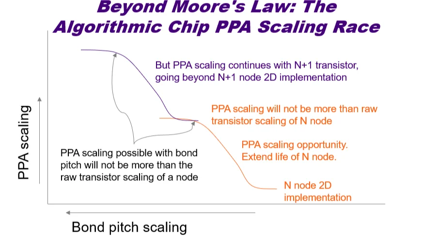
Beyond Moore’s Law: The Algorithmic Chip PPA Scaling Race That Was Already Underway
Image File
Original HTML

Beyond Moore’s Law: The Algorithmic Chip PPA Scaling Race That Was Already Underway

A recent semiconductor announcement has captured global attention — but the core ideas have deep roots in western academic research and design-methodology work across multiple firms, as reflected in public publications and patents.

Disclaimer: This article reflects the author’s personal professional perspective and is not intended to represent an official GlobalFoundries position. All technical references cited are publicly available. Any follow-up industry conversations will be coordinated consistent with GlobalFoundries policies.

The Announcement That Changed the Conversation

A semiconductor company’s “Tau Scaling Law” announcement in May 2026 introduced a new scaling framework — one that shifts attention from making transistors physically smaller to reducing signal delay across devices, circuits, chips, and systems. Coverage appeared in Reuters, CNBC, Nikkei Asia, Forbes, and The Register. Commentary has ranged from skeptical (“more branding than breakthrough”) to geopolitically significant (“a defining moment in the semiconductor bifurcation”).

Both reactions miss the deeper story.

The core thesis is straightforward: algorithmic and design-level scaling was not invented in 2026. What changed is the strategic importance of productizing it. The announcement is significant not because the concept is new, but because a design-driven scaling methodology is now being claimed as production-deployed across many chip variants.

In simple terms, Tau Scaling reframes chip scaling around time delay rather than geometry alone. Instead of relying primarily on smaller transistors, it seeks to reduce delay across devices, interconnects, circuits, chips, software, and systems through architecture, placement, routing, 3D integration, and hardware/software co-optimization.

The Western Footprint: Research That Was Always There

Consider two data points from the western technology ecosystem.

At the 2020 IEEE/ACM International Conference on Computer-Aided Design (ICCAD), researchers published a physical synthesis and post-layout optimization flow for monolithic design of 3D integrated circuits. The work demonstrated that stacking standard cells vertically — without shrinking the transistors themselves — could deliver up to 9 % smaller wirelength, 88 % improvement in timing slack, and 8.7 % lower power compared to conventional 2D designs. The core insight: better performance was achievable by changing how logic was spatially organized, not by demanding a new process generation from the foundry.

► "Pin-3D: A Physical Synthesis and Post-Layout Optimization Flow for Heterogeneous Monolithic 3D ICs," Proc. 39th ICCAD, ACM, Nov. 2020. DOI: 10.1145/3400302.3415720

A patent application filed with the United States Patent and Trademark Office in early 2024 covers a three-dimensional integrated circuit design methodology — specifically, how metal stack configuration and bonding pitch optimization interact to improve power, performance, and area (PPA). The approach describes two chips bonded face-to-face, with bonding pitch geometry directly driving PPA outcome.

► U.S. Patent Application No. 20250272465, “Three-Dimensional Integrated Circuit (3DIC) and 3DIC Design Method and System,” USPTO, filed February 2024. patents.google.com/patent/US20250272465A1

These are not isolated examples. They are representative of a sustained research and intellectual property trajectory in the western semiconductor ecosystem. The technical evidence comes from publications and patent filings; the broader strategic interpretation comes from industry analysis of how constraints change engineering priorities.

What Gets Built Under Pressure

A Forbes analysis published on Jun 27, 2026 frames this dynamic with precision. The author observes that “when best-in-class components are available externally, most firms source them externally. The cost of that efficiency is capability loss: they may never fully develop the internal muscle to align hardware, software, architecture and operations around one technical objective under pressure.”

► Mark Greeven, “What Huawei’s Chip Strategy Reveals About Innovation Under Pressure,” Forbes, June 27, 2026. forbes.com/sites/markgreeven/2026/06/27

This is the structural explanation for why the western ecosystem held the intellectual foundations — and did not build on them at scale. With access to extreme ultraviolet lithography and leading-edge foundry capacity, the path of least resistance was to let the transistor do the work. Algorithmic optimization was valuable as a complement to process scaling. It was not positioned, funded, or prioritized as a production-grade continuation of transistor scaling.

This is not a criticism, but a structural observation about how industries allocate attention and investment. When the dominant performance metric is transistor-based process-node progression, and when the supply chain reliably delivers new generations, the incentive to develop production-grade algorithmic alternatives is structurally limited.

The Forbes analysis adds a necessary nuance: constraint does not automatically create advantage — “more often, it creates delay, inefficiency, and technical debt” — and becomes strategically useful “only when an organization has enough engineering depth, resources, and market demand to convert constraint into discipline.” Productizing a complex design methodology across hundreds of chip variants over six years is exactly the kind of disciplined industrial execution that converts a research concept into a platform. Credit where it is due.

The Bifurcation Problem

The deeper concern is not whether any single company’s chip matches another’s on a specific benchmark. The deeper concern is what happens when export-constrained semiconductor ecosystems develop on divergent trajectories — different hardware, different software stacks, different EDA SW and methodologies, and importantly at different cost points.

The Forbes analysis identifies this directly: “Two AI compute ecosystems are now developing on separate trajectories, built on different hardware, different software stacks, different supply chains, and different assumptions.”

Recommended by LinkedIn

This bifurcation is visible in foundry market data. China’s share of advanced-node foundry revenue — which peaked near 30 % in 2019 — collapsed to approximately 12 % by 2025, driven by the cumulative effect of export control implementation. That collapse created precisely the industrial pressure that forced the algorithmic scaling path to production. The resulting ecosystem is now optimizing its software, models, and AI infrastructure around domestic hardware — not because it is superior by every metric, but because it is accessible.

As the Forbes analysis observes: “Adequacy within an accessible ecosystem can be worth more than optimality within one that is politically off-limits.”

For the global semiconductor industry, this is the inflection point. Algorithmic scaling approaches that improve PPA without requiring the next process node are no longer just a research direction. They are now being publicly claimed as production-scale methodologies — approaches that any ecosystem can study, adapt, and extend.

Why EDA and Algorithmic Solutions Were Structurally Underfunded

There is a structural reason why this class of solutions has not received investment commensurate with its technical potential.

Semiconductor technology leadership has historically been defined and communicated by materials science and device physics. Process roadmaps, conference keynotes, and investment theses are organized around the transistor as the atomic unit of progress. Electronic Design Automation (EDA) software and the algorithms that drive physical design have been positioned as infrastructure supporting the transistor’s trajectory — not as the lead driver of a parallel, and potentially complementary, scaling path.

The EDA industry has produced remarkable intellectual work for decades, while also carrying the burden of supporting the infrastructure required for leading transistor process-node scaling. When performance gains can be achieved by waiting for the next node, and when the supply chain reliably delivers new nodes, the business case for investing in production-grade algorithmic alternatives is structurally weaker. The research gets done in academic settings, but the investment to industrialize — to move from a compelling paper result to a commercial EDA flow — rarely follows at the same pace.

The result is a persistent gap between intellectual activity and commercial deployment. The 2020 ICCAD publication cited above, and the 2024 patent filing, both demonstrate that the western ecosystem was generating compelling work in this direction. What was missing was the industrial imperative to drive that work to production at scale.

What the Productization Moment Changes

The recent announcement changes the framing for the entire industry.

First, the EDA ecosystem has a clearer commercial signal. Supporting design-level scaling approaches is no longer a research bet. It is a demonstrated production requirement, with proven demand at volume across hundreds of chip variants.

Second, foundries that have invested in hybrid wafer bonding capability, fine-pitch interconnect technology, and 3D design-rule frameworks now have a more explicit value proposition for customers seeking performance beyond their current process node.

Third — and most urgently — the bifurcation problem makes this a strategic imperative. If the western ecosystem does not develop production-grade tools and methodologies for 3D monolithic design-driven scaling, it risks losing influence across key layers of the global semiconductor stack: silicon, IC design, software, and AI systems.

Class (B2B/B2C)
B2B
Ingest Status
Rewritten
Dedupe hash
06655f0ce525518d28a94e0ef2e58d41
Press Eligible
Yes
Press Eligible Reason
Manuelle Prüfung nötig. Risiko: MEDIUM. Flags: ['numbers']. Stichprobe: False
Source Name
GlobalFoundries Newsroom
Image URL
https://media.licdn.com/dms/image/v2/D5612AQHUEkjmtoYzXQ/article-cover_image-shrink_720_1280/B56Z8M54HWGcAQ-/0/1782627926719?e=2147483647&v=beta&t=FqJ63oayyH5epM61MvyjTgdwA8jQtogGQPX7fzEZ8p4
Content Hash (SHA-256, erste 32 hex)
33b13b42eb51760bcdae60ce88fb4f17
From Sand to Transistors: The Journey of Semiconductor Manufacturing
Image File
Original HTML

From Sand to Transistors: The Journey of Semiconductor Manufacturing

The semiconductor industry is at the heart of the technological revolution, it is projected to reach a market value of $1 trillion by 2030-2032. Yet, few realize that the foundation of these advanced microchips starts with something as simple as sand. The journey from raw silicon to functional transistors powering modern digital devices involves thousands of complex, high-precision steps carried out in ultra-clean environments.

Semiconductors begin with silicon, an element from the periodic table with atomic number 14, known for its ability to act as both a conductor and an insulator. It is the second most abundant element making up about 28% of Earth’s crust. Being both a conductor and an insulator, through a process called doping, impurities are introduced into silicon to control the flow of electricity, enabling the binary operations (0s - insulator and 1s - conductor) which are fundamental to digital computing.

The manufacturing process starts with refining sand to extract ultra-pure silicon free of any contaminants. This ensures that no unwanted elements interfere with the precision needed for chip fabrication. The purified silicon is melted at high temperatures and pressure and slowly cooled to form silicon ingots. These raw crystals of silicon are then sliced into thin silicon wafers and polished to a mirror-like finish to ensure precision in subsequent processing. These wafers come in different sizes, primarily measured by diameter. The semiconductor industry commonly uses wafers of 150mm (6 inches), 200mm (8 inches), and 300mm (12 inches), with the latter being the most widely used in modern manufacturing due to its efficiency in producing more chips per wafer. The thickness of these wafers varies between 0.7mm and 1mm, while their weight can range from 30g to 125g depending on the diameter.

Once the wafers are shaped, they undergo high-temperature oxidation in a furnace, reacting with oxygen to form an insulating layer of silicon dioxide, which protects the surface.

The next step, photo lithography, is similar to developing a photograph in a darkroom. The wafer is coated with a light-sensitive chemical, and a specialized machine projects UV light through a stencil-like photo-mask to create intricate circuit patterns. This step determines the blueprint of the microchip, much like how an architect’s blueprint guides the construction of a building. The wavelength of the light used in this process is critical, as it directly affects the resolution and miniaturization of transistors. Traditional deep ultraviolet (DUV) lithography uses 193 nm light sources, while extreme ultraviolet (EUV) lithography, operating at 13.5 nm, enables the production of advanced semiconductor nodes below 7 nm. The smaller the wavelength, the finer the detail that can be achieved, allowing for higher transistor density and improved performance in modern chips. These patterns are then refined through etching, which removes unwanted material to create the precise circuit structures. This step is crucial because it defines the intricate pathways that will allow transistors to function properly. Without precise etching, electrical signals could leak or short-circuit, leading to chip failure. Two techniques are used: wet etching, which dissolves materials using chemicals, and dry etching, which removes material with ionized gases for greater precision.

Deposition is the following step, adding functional layers using Chemical Vapor Deposition (CVD), which introduces gas-phase chemicals to form thin insulating or conductive layers, or Physical Vapor Deposition (PVD), which sprays atoms onto the wafer in a vacuum to form ultra-thin metal layers. These layers are essential for defining transistor behavior, controlling electrical flow, and ensuring reliability in high-performance computing. Ion implantation is then used to introduce impurities into the silicon, modifying its electrical properties. This step is fundamental in semiconductor design, as it allows the silicon to switch between conductive and insulating states, forming the basis of digital logic operations. Metallization deposits copper or aluminum layers, forming electrical pathways between transistors, effectively creating the nano 'wiring' that allows circuits to communicate. Without this step, transistors would remain isolated and unable to process or transfer information. Chemical Mechanical Polishing (CMP) ensures a smooth surface for optimal connectivity, preventing defects that could cause electrical resistance or signal loss.

All these steps are repeated multiple times to build the intricate layers of the electronic circuit pattern. The wafers are cleaned, between steps with high purity water to ensure no impurities are present on the surface, as these could jeopardize the chip's functioning.

Recommended by LinkedIn

Once the front-end processes are complete, wafers undergo rigorous electrical testing to verify circuit functionality before moving to the back-end phase. This stage focuses on transforming the processed wafer into a final semiconductor chip that can be integrated into electronic devices. Here, initial wafer testing filters out defective chips, followed by backlapping, which reduces wafer thickness, making chips more compact for modern devices.

After thinning, the wafer is diced into individual dies using precision cutting techniques such as laser cutting or mechanical sawing with high precision diamond saws. Each die is carefully handled to prevent damage and contamination, ensuring only fully functional chips proceed to the next stage they are subsequently packaged to protect their delicate structures while ensuring proper electrical connections.

Following dicing, each die undergoes die bonding, where it is securely attached to a substrate or package. Electrical connections are then made using either wire bonding, which involves connecting the chip to the package with fine metal wires, or flip-chip technology, which allows for direct connections to the circuit board.

Next, the chip is encapsulated in a protective casing, shielding it from mechanical stress and environmental factors. The final steps involve exhaustive testing, where chips are subjected to extreme conditions to ensure reliability—much like stress-testing a bridge before allowing traffic. Electrical, temperature, and stress tests confirm functionality, while burn-in tests simulate prolonged use to detect potential failures, ensuring that only the most robust chips reach the market.

The finished chips are then sorted, inspected, and prepared for shipment to be integrated into the latest consumer electronics, industrial machinery, and advanced computing systems.

The journey from sand to semiconductor is an extraordinary feat of human ingenuity, requiring precision engineering, cutting-edge physics, and global collaboration. Each microchip is the result of thousands of meticulous steps, reflecting the pinnacle of modern manufacturing.

Yet, no single company or country can manufacture a chip alone. The semiconductor value chain is one of the most interconnected industries in the world, spanning across continents—from raw material suppliers to fabrication plants, packaging, and testing facilities. A single microchip may contain components developed in the United States, front-end realized in Taiwan or South Korea, chemicals coming from Japan, tools and machinery from Netherland or the US and back end process done in Malaysia, and tested in Europe. And finally shipped all over the world. This level of global interdependence is what makes the industry both highly complex and increasingly influenced by geopolitical tensions.

The race for smaller, faster, and more efficient chips continues to push technological boundaries, but one thing remains unchanged: semiconductors are the product of a worldwide effort, where innovation is only possible through collaboration. As we step into an era dominated by artificial intelligence, quantum computing, and autonomous systems, the semiconductor industry will remain at the core of progress, proving that no great technological leap is ever made alone.

Next article: Semiconductor Value Chain

Very informative

Great overview! With EUV and chiplet architectures evolving, do you think the classic scaling process will still dominate in the next decade?

Great write up, Aymeric!

Great text Aymeric! I found the content very clear and it really simplifies the semiconductor process, making it much easier to understand, despite its inherent complexity.

Class (B2B/B2C)
B2B
Ingest Status
Rewritten
Dedupe hash
f8229506a0388249ccebf6c347e707a6
Press Eligible
Yes
Press Eligible Reason
Manuelle Prüfung nötig. Risiko: MEDIUM. Flags: ['finance', 'numbers']. Stichprobe: False
Source Name
GlobalFoundries Newsroom
Image URL
https://media.licdn.com/dms/image/v2/D5612AQFxVjbogEJ-zA/article-cover_image-shrink_423_752/B56ZUFxveYGsAc-/0/1739558681030?e=2147483647&v=beta&t=7NnXfoJOfTmRddrPnG7WteqPhEJCsLyhhYc6NRat4l4
Content Hash (SHA-256, erste 32 hex)
e83a395abd1f61d681a934d587098d39