Beyond Moore’s Law: The Algorithmic Chip PPA Scaling Race That Was Already Underway
A recent semiconductor announcement has captured global attention — but the core ideas have deep roots in western academic research and design-methodology work across multiple firms, as reflected in public publications and patents.
Disclaimer: This article reflects the author’s personal professional perspective and is not intended to represent an official GlobalFoundries position. All technical references cited are publicly available. Any follow-up industry conversations will be coordinated consistent with GlobalFoundries policies.
The Announcement That Changed the Conversation
A semiconductor company’s “Tau Scaling Law” announcement in May 2026 introduced a new scaling framework — one that shifts attention from making transistors physically smaller to reducing signal delay across devices, circuits, chips, and systems. Coverage appeared in Reuters, CNBC, Nikkei Asia, Forbes, and The Register. Commentary has ranged from skeptical (“more branding than breakthrough”) to geopolitically significant (“a defining moment in the semiconductor bifurcation”).
Both reactions miss the deeper story.
The core thesis is straightforward: algorithmic and design-level scaling was not invented in 2026. What changed is the strategic importance of productizing it. The announcement is significant not because the concept is new, but because a design-driven scaling methodology is now being claimed as production-deployed across many chip variants.
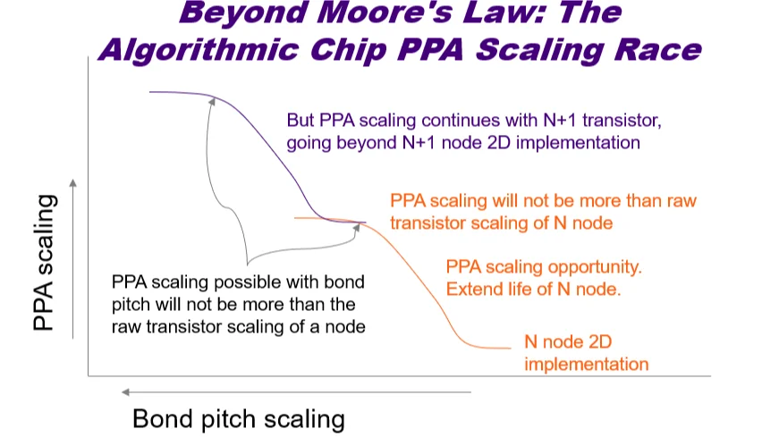
In simple terms, Tau Scaling reframes chip scaling around time delay rather than geometry alone. Instead of relying primarily on smaller transistors, it seeks to reduce delay across devices, interconnects, circuits, chips, software, and systems through architecture, placement, routing, 3D integration, and hardware/software co-optimization.
The Western Footprint: Research That Was Always There
Consider two data points from the western technology ecosystem.
At the 2020 IEEE/ACM International Conference on Computer-Aided Design (ICCAD), researchers published a physical synthesis and post-layout optimization flow for monolithic design of 3D integrated circuits. The work demonstrated that stacking standard cells vertically — without shrinking the transistors themselves — could deliver up to 9 % smaller wirelength, 88 % improvement in timing slack, and 8.7 % lower power compared to conventional 2D designs. The core insight: better performance was achievable by changing how logic was spatially organized, not by demanding a new process generation from the foundry.
► "Pin-3D: A Physical Synthesis and Post-Layout Optimization Flow for Heterogeneous Monolithic 3D ICs," Proc. 39th ICCAD, ACM, Nov. 2020. DOI: 10.1145/3400302.3415720
A patent application filed with the United States Patent and Trademark Office in early 2024 covers a three-dimensional integrated circuit design methodology — specifically, how metal stack configuration and bonding pitch optimization interact to improve power, performance, and area (PPA). The approach describes two chips bonded face-to-face, with bonding pitch geometry directly driving PPA outcome.
► U.S. Patent Application No. 20250272465, “Three-Dimensional Integrated Circuit (3DIC) and 3DIC Design Method and System,” USPTO, filed February 2024. patents.google.com/patent/US20250272465A1
These are not isolated examples. They are representative of a sustained research and intellectual property trajectory in the western semiconductor ecosystem. The technical evidence comes from publications and patent filings; the broader strategic interpretation comes from industry analysis of how constraints change engineering priorities.
What Gets Built Under Pressure
A Forbes analysis published on Jun 27, 2026 frames this dynamic with precision. The author observes that “when best-in-class components are available externally, most firms source them externally. The cost of that efficiency is capability loss: they may never fully develop the internal muscle to align hardware, software, architecture and operations around one technical objective under pressure.”
► Mark Greeven, “What Huawei’s Chip Strategy Reveals About Innovation Under Pressure,” Forbes, June 27, 2026. forbes.com/sites/markgreeven/2026/06/27
This is the structural explanation for why the western ecosystem held the intellectual foundations — and did not build on them at scale. With access to extreme ultraviolet lithography and leading-edge foundry capacity, the path of least resistance was to let the transistor do the work. Algorithmic optimization was valuable as a complement to process scaling. It was not positioned, funded, or prioritized as a production-grade continuation of transistor scaling.
This is not a criticism, but a structural observation about how industries allocate attention and investment. When the dominant performance metric is transistor-based process-node progression, and when the supply chain reliably delivers new generations, the incentive to develop production-grade algorithmic alternatives is structurally limited.
The Forbes analysis adds a necessary nuance: constraint does not automatically create advantage — “more often, it creates delay, inefficiency, and technical debt” — and becomes strategically useful “only when an organization has enough engineering depth, resources, and market demand to convert constraint into discipline.” Productizing a complex design methodology across hundreds of chip variants over six years is exactly the kind of disciplined industrial execution that converts a research concept into a platform. Credit where it is due.
The Bifurcation Problem
The deeper concern is not whether any single company’s chip matches another’s on a specific benchmark. The deeper concern is what happens when export-constrained semiconductor ecosystems develop on divergent trajectories — different hardware, different software stacks, different EDA SW and methodologies, and importantly at different cost points.
The Forbes analysis identifies this directly: “Two AI compute ecosystems are now developing on separate trajectories, built on different hardware, different software stacks, different supply chains, and different assumptions.”
Recommended by LinkedIn
This bifurcation is visible in foundry market data. China’s share of advanced-node foundry revenue — which peaked near 30 % in 2019 — collapsed to approximately 12 % by 2025, driven by the cumulative effect of export control implementation. That collapse created precisely the industrial pressure that forced the algorithmic scaling path to production. The resulting ecosystem is now optimizing its software, models, and AI infrastructure around domestic hardware — not because it is superior by every metric, but because it is accessible.
As the Forbes analysis observes: “Adequacy within an accessible ecosystem can be worth more than optimality within one that is politically off-limits.”
For the global semiconductor industry, this is the inflection point. Algorithmic scaling approaches that improve PPA without requiring the next process node are no longer just a research direction. They are now being publicly claimed as production-scale methodologies — approaches that any ecosystem can study, adapt, and extend.
Why EDA and Algorithmic Solutions Were Structurally Underfunded
There is a structural reason why this class of solutions has not received investment commensurate with its technical potential.
Semiconductor technology leadership has historically been defined and communicated by materials science and device physics. Process roadmaps, conference keynotes, and investment theses are organized around the transistor as the atomic unit of progress. Electronic Design Automation (EDA) software and the algorithms that drive physical design have been positioned as infrastructure supporting the transistor’s trajectory — not as the lead driver of a parallel, and potentially complementary, scaling path.
The EDA industry has produced remarkable intellectual work for decades, while also carrying the burden of supporting the infrastructure required for leading transistor process-node scaling. When performance gains can be achieved by waiting for the next node, and when the supply chain reliably delivers new nodes, the business case for investing in production-grade algorithmic alternatives is structurally weaker. The research gets done in academic settings, but the investment to industrialize — to move from a compelling paper result to a commercial EDA flow — rarely follows at the same pace.
The result is a persistent gap between intellectual activity and commercial deployment. The 2020 ICCAD publication cited above, and the 2024 patent filing, both demonstrate that the western ecosystem was generating compelling work in this direction. What was missing was the industrial imperative to drive that work to production at scale.
What the Productization Moment Changes
The recent announcement changes the framing for the entire industry.
First, the EDA ecosystem has a clearer commercial signal. Supporting design-level scaling approaches is no longer a research bet. It is a demonstrated production requirement, with proven demand at volume across hundreds of chip variants.
Second, foundries that have invested in hybrid wafer bonding capability, fine-pitch interconnect technology, and 3D design-rule frameworks now have a more explicit value proposition for customers seeking performance beyond their current process node.
Third — and most urgently — the bifurcation problem makes this a strategic imperative. If the western ecosystem does not develop production-grade tools and methodologies for 3D monolithic design-driven scaling, it risks losing influence across key layers of the global semiconductor stack: silicon, IC design, software, and AI systems.