Garmin International, Inc. News
Image File
Original HTML

The ultimate smartwatch

Our most advanced golf smartwatch

Premium cycling computer with hands-free voice control

Powerful smart trainer with multidirectional motion

The ultimate smartwatch

Ultraperformance GPS smartwatch

Simplify your drive with new ultrawide displays

See real-time digital flag signals in the cockpit

Racing radar for high-performance drivers and track enthusiasts

Advanced marine head units

Our clearest sonar ever

Integrated flight displays for experimental and certified piston aircraft

Ultimate aviator smartwatch with satellite and LTE connectivity

Class (B2B/B2C)
Ignore
Ingest Status
Rejected
Dedupe hash
d51761d0df383062ffefe65182088a9c
Press Eligible
No
Press Eligible Reason
Text too short (78 words. Min: 150)
Source Name
Garmin International, Inc.
Image URL
https://res.garmin.com/en/products/010-03899-00/v/cf-lg.jpg
Content Hash (SHA-256, erste 32 hex)
255d2b33a1ed7c088fa4f69c9f84807b
We Just Can’t Wait! Be Prepared! New Details for Lion King Ride Coming to Disneyland Paris
Image File
Original HTML

Be Prepared!

- Construction is now underway on the first-ever immersive world themed to Walt Disney Animation Studios’ The Lion King at Disney Adventure World.

- An all-new major attraction will delight guests with iconic moments and songs from the 1994 animated film.

- Audio-Animatronics figures, special effects, and three exciting slopes will bring the story of the film to life.

Have you been looking for even more details about the brand-new attraction themed around Simba and the rest of the animal kingdom coming to Disneyland Paris? Hakuna matata; it’s our problem-free philosophy and we’ve got you covered!

Lion King Ride to Feature Iconic Songs and Scenes

When the sun rises on the realm after the exciting debut of this highly-anticipated attraction, you’ll be invited into an area of Disney Adventure World dedicated exclusively to Walt Disney Animation Studios’ The Lion King to experience an all-new water attraction that will plunge guests deep into the heart of the Pride Lands, complete with iconic songs from the 1994 masterpiece.

After making your way to the caves beneath the 120-foot-high Pride Rock, you will take your own place in the Circle of Life when you embark on a sensational and musical adventure, listening to classic songs and passing through a variety of memorable scenes from the film, including Simba’s final confrontation with Scar. The new ride is a full retelling of Simba’s journey from cub to king, detailing the happy times… and the not-so-happy times that stood in the way of the future king of Pride Rock.

Once the attractions roars to life, it will be one of the largest attractions at the resort, featuring a new flume system and a thrilling 52-foot drop. The new ride will be featured in an all-new immersive world dedicated to the characters and stories from the film, with plenty of dining, shopping, and opportunities to meet some favorite characters.

Construction has already begun following the debut of Disney Adventure World earlier this year, and this new attraction and area of the park will be a major piece of the creative vision included in the ongoing transformation of the second park at Disneyland Paris.

For even more information on the full lineup of new experiences coming to Disneyland Paris and beyond, check out the latest updates from D23 on the Disney Parks Blog, including new updates coming soon to Space Mountain.

Watch out for even more updates in the future and remember… remember… remember to follow along on the Disney Parks Blog for more!

Class (B2B/B2C)
B2C
Ingest Status
Rewritten
Dedupe hash
e546d9faec3a4bc1ba77ce13e246eec8
Press Eligible
Yes
Press Eligible Reason
Disneyland Paris attraction and guest experience announcement.
Source Name
Disney Parks Blog
Image URL
https://disneyparksblog.com/app/uploads/2026/08/Lion-King-Attraction-Scar.png
Source Node
Content Hash (SHA-256, erste 32 hex)
ece09916d89f383ace883d27f20e65d1
Disney Cruise Line Shares First Look at New Class of Ships
Image File
Original HTML

Let’s see… you’ve got Disney Magic, and Disney Fantasy. And Disney Dream and Disney Wonder. And after that comes Disney Wish, Disney Treasure, and Disney Destiny. Then Disney Adventure! And coming soon, Disney Believe. But then what comes next? The Disney Experiences Showcase, Horizons: A Carousel of Progress gave a sneak peek at the entirely new class of ships Disney Cruise Line will debut in 2029.

Announced during D23: The Ultimate Disney Fan Event presented by Visa back in 2024, Disney Cruise Line is expanding its fleet to 13 over the coming years. The Disney Believe, setting sail in 2027, will be the fourth ship in the Wish class. After that, it’s time for a new story at sea with the launch of three new ships in a brand-new class.

Claire Weiss joined host Neil Patrick Harris (and Jack McBrayer dressed as Captain Jack Sparrow, but that’s a story for another day) to talk about the new ships.

While details are still locked away in a treasure chest, Claire revealed that these three ships will introduce an entirely new class to the fleet and occupy a unique place in Disney Cruise Line’s growing lineup. Positioned in size between Disney’s classic ships and its newer vessels, this class opens the door to exciting possibilities for future itineraries and experiences around the globe.

As Claire explained to the crowd, these new ships are “right in the middle of our classic ships and our newer ones. That gives us some amazing opportunities to visit new places and reach brand new audiences we haven’t before.” For those unfamiliar with the size and scale of a Disney Cruise Line ship, that translates to bigger than the Disney Wonder, but smaller than the Disney Wish!

That sweet spot in size gives Disney Cruise Line even more flexibility as it continues to grow around the world, bringing unforgettable vacations to new destinations and welcoming even more families aboard. While we’ll have to wait a little longer to learn more about these ships and the adventures they’ll offer, fans at the showcase were treated to something special: the very first preview of the new class.

And when we say first look, we mean it. Claire revealed that the teaser shown during the presentation had never been seen publicly before, giving the audience an exclusive glimpse at the future of Disney Cruise Line. Sail into the first look below.

What are the Disney Cruise Line Ships?

With the announcement of an all-new class of ships on the horizon (no pun intended), now is the perfect time to take a look at the ships that make up the Disney Cruise Line fleet. Currently, Disney Cruise Line sails eight ships across the world. Each ship brings its own unique personality while delivering the legendary Disney storytelling, entertainment, dining, and service guests know and love.

- Disney Magic and Disney Wonder

- The ships that started it all, that introduced Disney Cruise Line’s signature blend of classic ocean liner elegance and Disney storytelling. These ships offer a more intimate feel while still delivering fan-favorite experiences, enchanting entertainment, and plenty of pixie dust around every corner.

- Disney Dream and Disney Fantasy

- Designed to bring even more magic to the high seas, the Disney Dream and Disney Fantasy expanded the Disney Cruise Line experience with larger ships, innovative dining concepts, and immersive spaces inspired by favorite Disney stories. These ships are known for their grand atriums, family-friendly fun, and unforgettable entertainment from bow to stern.

- Disney Wish, Disney Treasure, Disney Destiny, and Disney Believe

- Inspired by the power of wishes and Disney storytelling, the newest ships take guests on adventures filled with beloved characters, immersive experiences, and beautifully themed spaces. Each ship in the class celebrates a different spirit of Disney storytelling while offering innovative dining, spectacular entertainment, and plenty of magical surprises along the way.

- Disney Adventure

- The most recently launched Disney Cruise Line ship, the Disney Adventure brings even more Disney magic to families around the world. The ship, which sails from Singapore, introduces exciting new experiences, larger-than-life entertainment, and imaginative spaces inspired by beloved Disney, Pixar, and Marvel stories, creating unforgettable adventures for families across Southeast Asia.

Class (B2B/B2C)
B2C
Ingest Status
Rewritten
Dedupe hash
fe7f19be924839a45ead24c288513450
Press Eligible
Yes
Press Eligible Reason
Disney announces a new class of cruise ships and fleet expansion for family travelers.
Source Name
Disney Parks Blog
Image URL
https://disneyparksblog.com/app/uploads/2026/08/1M0A2257-scaled.jpg
Source Node
Content Hash (SHA-256, erste 32 hex)
450e1eb16849c939b65632dd92b7cd88
Monstropolis at Disney World: News from D23 2026
Image File
Original HTML

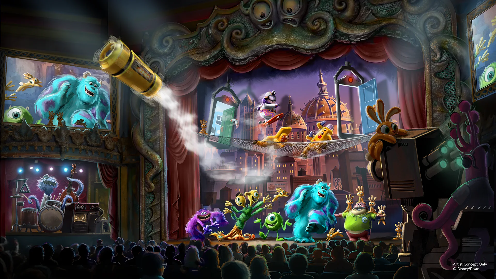
Today during “Horizons: A Carousel of Progress” at D23: The Ultimate Disney Fan Event presented by Visa, Neil Patrick Harris brought a few special guests out to tell us about the new sights coming soon to Monstropolis at Disney’s Hollywood Studios.

“Welcome to Monstropolis,” written by Disney Legend, Randy Newman, is the first song that Randy has composed for a Disney theme park, and you’ll hear it next year when Monstropolis opens to humans.

That’s right, while work continues on the door coaster, parts of Monstropolis will open to guests in 2027. Michael Hundgen, Vice President Creative, and Chris Beatty, Vice President, Walt Disney Imagineering, were played onto the stage to talk about the dynamic moments and locations you’d expect to see in Monstropolis.

Glob Theater

Chris explained that humans are invited to attend a new show at the Glob Theater, titled “Welcome to Monstropolis,” just like Randy Newman’s new song.

Chris revealed that the monsters in the show will introduce humans to Monstropolis , and highlight how similar monsters and humans really are.

“Mike and Sulley will be our hosts,” Chris said. “Sulley has been working on a small, homespun show, but Mike – ever the showman – has a few surprises up his sleeve that he thinks will bring down the house. Hopefully not literally.”

What could go wrong?

Archie’s Scare Pig Pizza

People and monsters all love pizza, and Monstropolis’ top-rated pizza will be your go-to place to grab a slice. Humans may recognize Archie, Fear Tech’s beloved six-legged mascot, but after years of being “borrowed” by mischievous MU students, he’s become a fan favorite on both campuses.

Next door, the Monsters University Alumni Club has also opened its doors to human visitors eating at Archie’s.

Monsters University Alumni Club

Head on down for a who’s who of all the student clubs, fraternities, and sororities at MU. Chris said you’ll even find a tribute worth browsing. “Inside the Alumni Club is the elite Scarer’s Club, honoring the school’s legendary scarers from years past.”

Scareporium

And you’ll want a little something to commemorate your visit to Monstropolis. The Scareporium, as Chris said, will be, “… a shop where all of us human tourists can grab a great souvenir to remember our visit.”

Harryhausen’s Restaurant

Michael also showed off the dining location we have all been waiting for, the location of one of Mike and Celia’s most unforgettable dates.

With a new menu to lay your eyes on (whether you have one, two, or ten), a visit to Harryhausen’s will spotlight the famed sushi chef, brought to life here as a new Audio-Animatronics figure. Watch his many tentacles whip up delicious-looking Monster-worthy creations, but don’t worry, there’s more than just sushi on the menu.

Michael said that it will be, “A menu unlike anything else we offer at Walt Disney World. It will be a great place to bring your Schmoopsie-poo for a romantic meal.”

Discovering Monstropolis at Walt Disney World

Monstropolis is starting to take shape as construction continues at Disney’s Hollywood Studios in Walt Disney World Resort! Steel rises behind the walls, new details emerge almost daily, and with every milestone, the world of Disney and Pixar’s Monsters, Inc. is roaring to life. Through a creative collaboration between Walt Disney Imagineering and Pixar Animation Studios, guests will finally be able to take in all the monstrous sights, tastes, and sounds of Sulley and Mike’s world.

But this isn’t just a new land taking shape, it’s the beginning of a new story.

Monstropolis — the monster city now powered by laughter — is getting ready to give humans a glimpse of what’s been hidden from their world for generations. Which raises an interesting question: if humans were never meant to enter the monster world … why are the doors finally opening to us?

As it turns out, the answer is already making headlines in the city of Monstropolis. Through the pages of the Monstropolis Horn, the city’s official newspaper, monsters are talking about a “historic decision” that’s about to seriously mix things up for monster kind.

A Laugh That Changed It All

For generations, Monstropolis ran on fear, and not just because the monsters used screams to power their society: monsters were scared of us, too! Humans were seen as dangerous, toxic, and completely off-limits. I mean, who could forget the decontamination protocols for a 2319?!

When James P. Sullivan and Mike Wazowski (you know, with one eye) discovered that human laughter generates far more power than screams, it didn’t just transform the energy crisis, it transformed Monstropolis itself. Fear gave way to curiosity. Caution gave way to connection. And for the first time, the doors separating the monster world from ours no longer felt like barriers.

What started as a breakthrough inside Monsters, Inc. quickly became something much bigger: a citywide shift in how monsters viewed humans. Scales fell from their eyes – well, at least for the monsters with scales to shed.

Enter: The Department of Human Relations

As Monstropolis evolved, so did its connection with the human world. You may have heard of the HR department, but you haven’t heard of this HR department … that’s right, I’m talking about the Department of Human Relations. This new team established by the city has been tasked with sinking their teeth – and in some cases, their very BIG teeth – into helping monsters better understand humans as welcomed guests.

The newly instated department has been spearheading a moment that was once thought impossible: inviting humans into Monstropolis for the very first time. And that invitation has a name.

H.U.M.A.N. Day: A Celebration with a Purpose

H.U.M.A.N. Day, short for “Humans Understanding Monsters Are Nice,” marks a historic milestone for the city. Part celebration, part cultural exchange, the event is designed to introduce humans to life inside Monstropolis while helping monsters discover that humans are not so frightening after all. Now that’s something to snarl – ahem, smile about!

Human guests will have the chance to explore the city, meet its citizens, taste unique cuisine, and step into the everyday world of monsters in a totally new way. For the first time, two worlds once separated are meeting face to scaly, furry, and fang-filled face – brought together not by screams, but by laughter.

Exploring the Streets of Monstropolis

As more of Monstropolis comes into view, one thing is clear: move over, cities of the human world! Monstropolis is going to be the next big vacation destination!

Storefronts line the streets, industries hum alongside everyday life, and every corner reflects the quirky, character-filled world fans fell in love with. And of course, it wouldn’t be Monstropolis without a few iconic stops along the way. Places like Harryhausen’s — yes, THAT legendary restaurant monsters line up for — and the Glob Theater help bring the city to life, adding even more personality, energy, and can’t-miss moments around every corner.

There’s still plenty more to uncover, so keep an eye or two (or six or eight!) on the Disney Parks Blog for more details as Monstropolis gets ready to roll out the welcome mat on H.U.M.A.N. Day in 2027.

Class (B2B/B2C)
B2C
Ingest Status
Rewritten
Dedupe hash
980ad8fc2a759ac8cd7dff44e85096b2
Press Eligible
Yes
Press Eligible Reason
Disney announces upcoming attractions, dining, and experiences at Walt Disney World.
Source Name
Disney Parks Blog
Image URL
https://disneyparksblog.com/app/uploads/2026/08/Glob-Theater_Monstropolis.png
Source Node
Content Hash (SHA-256, erste 32 hex)
4adcc08718baa320c84dda5f0938203b
Understanding the Semiconductor Value Chain: From Design to End Products
Image File
Original HTML

Understanding the Semiconductor Value Chain: From Design to End Products

The semiconductor industry is at the heart of modern technology, powering everything from smartphones to electric vehicles and advanced computing systems. Yet, the journey of a semiconductor chip from conception to final integration into an electronic device is an intricate process involving multiple specialized players.

The semiconductor value chain consists of several key categories: Design (IP), Electronic Design Automation (EDA), Fabless Design, Foundries & OSAT, Integrated Device Manufacturers (IDM), Chemical & Wafer suppliers, Equipment manufacturers, and finally, the companies that integrate semiconductors into electronic products.

Understanding how these different segments interact is crucial to appreciating the complexity and innovation behind the devices we use every day.

Design (IP) – The Foundation of Innovation

At the core of semiconductor development is Intellectual Property (IP) design. Semiconductor design companies create the blueprints for chips that define their functionality and performance. These designs include complex layouts of transistors and logic circuits optimized for power efficiency, processing speed, and specialized applications such as AI, 5G, or IoT. Some of the most critical semiconductor IPs are developed by companies such as ARM, Imagination, which license their technology to chipmakers worldwide. Emerging players are also making an impact by focusing on open-source architectures and energy-efficient designs. The growing complexity of chip design is leading to a rise in demand for IP customization, where companies are tailoring solutions to meet specific application needs, such as high-performance computing or low-power IoT devices.

Electronic Design Automation (EDA) – The Tools That Enable Complexity

Given the extreme complexity of modern semiconductor designs, engineers rely on specialized software tools known as Electronic Design Automation (EDA) to create, simulate, and verify chip designs before manufacturing. EDA tools help engineers model circuits, optimize performance, and ensure that a design can be manufactured efficiently in a factory. Industry leaders such as Synopsys, Cadence, and Siemens EDA provide these essential tools, enabling the entire semiconductor ecosystem to function at the cutting edge. Continuous innovation in AI-driven chip design is also transforming the way semiconductors are developed, reducing time to market and improving efficiency. The growing adoption of cloud-based EDA tools is further revolutionizing the industry, allowing global teams to collaborate seamlessly on chip development.

Fabless Design – The Architects of Semiconductor Innovation

Many of the world's most well-known semiconductor companies, including NVIDIA, Qualcomm, and AMD, follow a fabless business model, meaning they design and market chips but do not own manufacturing facilities. Instead, they focus on developing high-performance processors, graphics units, and specialized chips, outsourcing the actual fabrication to foundries. This model allows them to concentrate on innovation without the high capital investment required for semiconductor manufacturing. The rise of AI and machine learning applications has led to a growing demand for customized chips, further driving innovation in the fabless sector. Additionally, startups focusing on application-specific integrated circuits (ASICs) and domain-specific architectures are gaining traction, offering optimized solutions for AI, 5G, and automotive industries. Some major manufacturers of electronic products now have teams designing their own chips as well to ensure their requirements are properly met.

Foundries & OSAT – The Makers of Silicon

Foundries are the front-end facilities that manufacture semiconductor chips based on the designs provided by fabless companies or outsourced by IDMs. Leading foundries such as TSMC, Samsung Foundry, United Microelectronics Corporation, and GlobalFoundries use advanced lithography techniques to produce cutting-edge semiconductors. Because chip fabrication is a highly sophisticated and capital-intensive process, foundries operate at an enormous scale, producing millions of chips with nanometer precision.

Recommended by LinkedIn

Once chips are manufactured, they must be tested and packaged before they can be integrated into final products. Outsourced Semiconductor Assembly and Test (OSAT) companies (back-end process), such as ASE, Amkor, and JCET, handle these processes, ensuring that each chip meets rigorous quality standards before it is shipped to electronic manufacturers. As demand increases for advanced packaging techniques, OSAT companies are playing an even more critical role in enhancing semiconductor performance. The rise of 3D packaging and chiplet-based architectures is pushing OSAT firms to develop innovative assembly methods that improve efficiency and performance.

Integrated Device Manufacturers (IDM) – Combining Design and Production

Unlike fabless companies, Integrated Device Manufacturers (IDMs) own both the design and manufacturing operations, giving them end-to-end control over semiconductor production. Companies such as Intel, Samsung, and Texas Instruments follow the IDM model, which allows them to tailor their manufacturing processes to optimize performance for their specific chip designs. This vertical integration enables them to innovate rapidly and maintain high levels of quality and security throughout production. IDMs are also investing in expanding their fabrication capacity to reduce reliance on external foundries and ensure a more resilient supply chain. Recent trends show IDMs increasingly collaborating with third-party foundries for specific process nodes, balancing flexibility with in-house production.

Chemical & Wafer Suppliers – The Raw Materials of Semiconductors

Semiconductor manufacturing requires highly specialized raw materials, particularly silicon wafers and various chemicals used in photolithography, etching, and deposition processes. Companies like Shin-Etsu Chemical, Sumco, and GlobalWafers produce ultra-pure silicon wafers, while others supply high-performance gases, resists, and solvents essential for chip fabrication. The precision and purity of these materials are critical for ensuring that semiconductor manufacturing processes meet the highest standards of performance and reliability. As sustainability concerns grow, many suppliers are investing in greener and more efficient production methods, including recycling chemicals and reducing water usage in wafer production.

Equipment Manufacturers – The Enablers of Advanced Fabrication

Building semiconductor chips requires some of the most advanced equipment in the world. Companies such as ASML, Applied Materials, and Lam Research provide the lithography machines, etching systems, and deposition tools that make high-performance chip manufacturing possible. ASML’s extreme ultraviolet (EUV) lithography machines, for example, are essential for producing the most advanced chips at 3nm and beyond. Innovations in semiconductor equipment help extend Moore’s Law, producing faster, more efficient chips with each new generation. Investment in new fabrication technologies, such as high-NA EUV and quantum computing materials, is expected to drive the next wave of semiconductor advancements.

Manufacturers of Electronic Products – Bringing Chips to Consumers

Finally, semiconductor chips are integrated into electronic devices by manufacturers such as Tesla, Bosch, Siemens, Haier, and Schneider Electric. These companies design products that leverage semiconductor technology to create electric vehicles, industrial automation systems, medical devices, and more. The growing demand for AI, IoT, and autonomous systems is further driving the need for specialized semiconductor solutions, particularly in edge computing and real-time processing applications.

Global Cooperation – A Necessity for the Semiconductor Industry

The semiconductor value chain is a prime example of global interdependence. No single country or company can master every aspect of chip design, manufacturing, and equipment production. Instead, different regions have developed specialized expertise, while emerging players, backed by substantial government funding, are making strides to close the technology gap and establish themselves in the industry. The value chain is also evolving, with significant shifts on the horizon. ARM is set to debut its first in-house chip by summer, signaling a move beyond its traditional role as an IP provider and into chip design. Meanwhile, Intel's future remains uncertain following the departure of CEO Pat Gelsinger in December 2024, raising questions about the company’s long-term strategy as an IDM and competitiveness. At the same time, startups are making significant investments in specialized areas of the value chain, introducing innovations that could disrupt the industry's traditional dynamics.

To ensure a stable and resilient supply chain, international cooperation and strategic partnerships are essential. The industry’s complexity and capital intensity make it impossible for any nation or company to go at it alone. Attempts at full vertical integration remain unrealistic in the near term, reinforcing the need for alignment across borders. Challenges such as geopolitical tensions, supply chain disruptions, and sustainability concerns will continue to shape the industry's future. Without global collaboration, the semiconductor industry's progress, economic stability, and technological leadership could be at risk. Only through strengthened international partnerships can the sector ensure long-term resilience, innovation, and sustainability.

Quite impressive landscape we seldom see so clearly. Thanks for this journey sir :) In our digital world, semiconductors business occupies a central place.

Class (B2B/B2C)
B2B
Ingest Status
Rewritten
Dedupe hash
021590ba16f7fee8d407fc275f74f5ab
Press Eligible
Yes
Press Eligible Reason
Manuelle Prüfung nötig. Risiko: MEDIUM. Flags: ['numbers']. Stichprobe: False
Source Name
GlobalFoundries Newsroom
Image URL
https://media.licdn.com/dms/image/v2/D5612AQEmw6Di3iP2-g/article-cover_image-shrink_720_1280/B56ZUn9BcJGUAI-/0/1740132064341?e=2147483647&v=beta&t=e-WNitjr7WrCcZ9dVCWqzgsETTo-Z2nr_UgJ3Bch3CA
Content Hash (SHA-256, erste 32 hex)
a2d63d71d953d202d690c16a6e496dae
Can GlobalFoundries Seize the Moment After TSMC's Exit to Forge a New GaN Market Landscape?
Image File
Original HTML

Can GlobalFoundries Seize the Moment After TSMC's Exit to Forge a New GaN Market Landscape?

Introduction: A Confluence of Strategy, Policy, and Opportunity

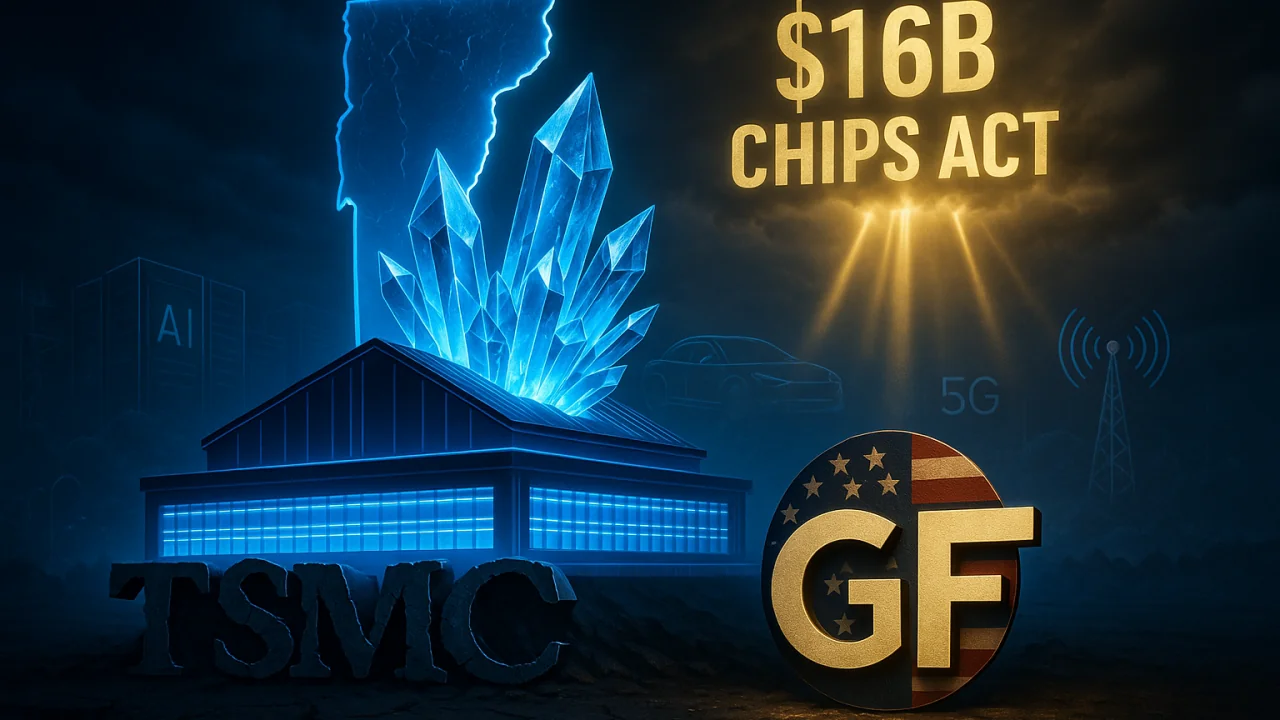
On June 4, 2025, a landmark announcement signaled a major realignment in the American semiconductor landscape. GlobalFoundries (GF), the largest U.S.-based foundry, unveiled a monumental $16 billion investment to expand its manufacturing and advanced packaging capabilities in New York and Vermont. Backed by a consortium of tech titans including Apple, SpaceX, AMD, Qualcomm, NXP, and General Motors, this is no mere capacity expansion. It is a strategic maneuver aimed at rebuilding domestic semiconductor prowess in AI, energy-efficient computing, and communications infrastructure, directly addressing America's reliance on foreign supply chains for critical technologies.

This move is best understood as a pilot for a new era of "government-business collaboration." GF has been tasked with spearheading national priorities, including silicon photonics for data centers, FDX processes for edge AI, and, most critically, next-generation GaN power solutions. The Vermont facility, in particular, has been designated as the core hub for GaN technology development, positioning it as a lynchpin in the U.S. government's strategy to re-architect the power semiconductor ecosystem.

The timing is uncanny. Just one month after GF's declaration, TSMC confirmed its plan to exit the GaN foundry business by 2027. This created an immediate and urgent vacuum, amplifying the need for a robust "domestic alternative." GF's proactive deployment appears as a perfectly timed strategic response—a calculated move to both capture a vital position in the third-generation semiconductor race and align with powerful geopolitical and policy tailwinds.

This article will deconstruct how GF's GaN business evolved from a peripheral exploration into a central strategic pillar. We will analyze this transformation within the intricate context of the global GaN foundry map, shifting supply chains, technological evolution, and geopolitical chess. Ultimately, we seek to answer a more profound question: In the wake of TSMC's departure, what kind of Wide-Bandgap (WBG) semiconductor ecosystem is the United States truly determined to build?

🔷 Chapter 1: The CHIPS Act and the Dawn of a New Opportunity

To grasp GlobalFoundries' GaN ambitions, one must first understand the seismic policy shift driven by the CHIPS and Science Act. This legislation, coupled with GF's unique strategic posture, has created an unprecedented historical window for the company to emerge as a leader in the GaN arena.

■ The Deep Strategic Intent of the CHIPS Act

Signed into law in 2022, the CHIPS Act represents the most significant U.S. government intervention in the semiconductor industry since the Cold War. Authorizing approximately $280 billion, its goal is to reassert American leadership across the semiconductor value chain.

Of the total, $52.7 billion is allocated directly to support the U.S. semiconductor industry, with the breakdown as follows:

$39 billion for domestic semiconductor manufacturing, including both advanced and mature technologies.

$13.2 billion for research and workforce development.

Additionally, the Act introduced a $24 billion investment tax credit (ITC), offering a powerful 25% credit on qualified capital expenditures for semiconductor facilities in the U.S.

Crucially, the Act embeds "national security guardrails," revealing its geopolitical underpinnings:

Technology Clawback: Prohibits recipients from engaging in joint R&D or technology licensing with "foreign entities of concern," primarily targeting China.

Expansion Restrictions: Forbids subsidized companies from expanding advanced semiconductor manufacturing in designated countries, including China, for a decade.

The policy's essence is clear: to forge a "U.S.-centric, geopolitically secure" semiconductor supply chain through a potent combination of financial incentives and strategic restrictions.

■ GlobalFoundries: The Chosen Champion and Its Policy Advantages

In this state-driven industrial reconfiguration, GlobalFoundries is a prime beneficiary. As America's largest pure-play foundry, its strategic importance to national defense and communications infrastructure makes it a natural strategic partner.

GF has been awarded $1.5 billion in direct federal funding from the CHIPS Act to expand its Fab 8 facility in Malta, New York. Additionally, the state of New York provided $575 million in matching funds. Yet, the more telling move is in Vermont. The Essex Junction facility (Fab 9), a former IBM asset, has been given a renewed, critical mission:

"Trusted Foundry" Designation: Fab 9 is a DoD-certified Trusted Foundry, responsible for producing mission-critical chips for aerospace and military communications. This trusted status is non-negotiable for national security applications.

GaN-on-Si Development Hub: The Vermont plant is now the designated center for GF's GaN power and RF chip development. Leveraging its existing 200mm CMOS platform, GF is building a GaN-on-Si process designed for seamless compatibility with its 180nm workflows.

Even before the main CHIPS Act funding, the U.S. government had been nurturing GF's GaN capabilities, providing over $85 million between 2020 and 2023 for platform development. This pattern of "early strategic backing + ongoing targeted investment" unequivocally signals the government's view of GF as a cornerstone of its "trusted GaN process chain."

🔷 Chapter 2: GF's GaN Journey – From Policy-Driven Exploration to National Strategy

Unlike TSMC's market-driven, decade-long accumulation of GaN expertise, GlobalFoundries' path is a textbook case of "policy-driven" technology incubation. It began with government-seeded R&D, evolved through small-scale prototyping, and is now being catapulted to industrial scale by national-level resources like the CHIPS Act. This is a classic "government-demand pull + in-house platform evolution" model.

■ A History of Differentiation: GF's Strategic DNA

Founded in 2009 as a spin-off from AMD and expanded in 2015 with the acquisition of IBM's microelectronics business, GF's history is one of strategic transformation. By the end of 2024, it stood as a global foundry leader with $6.75 billion in 2024 revenue and wafer shipments totaling 2.1 million (300mm equivalent).

A pivotal moment in its history was the decision to exit the "arms race" for bleeding-edge logic (7nm and below). Instead, GF focused its resources on differentiated technologies. This prescient move made it the ideal candidate to champion national strategic initiatives when the CHIPS Act wave arrived.

■ The Genesis of GaN: A Government-Sponsored Exploration

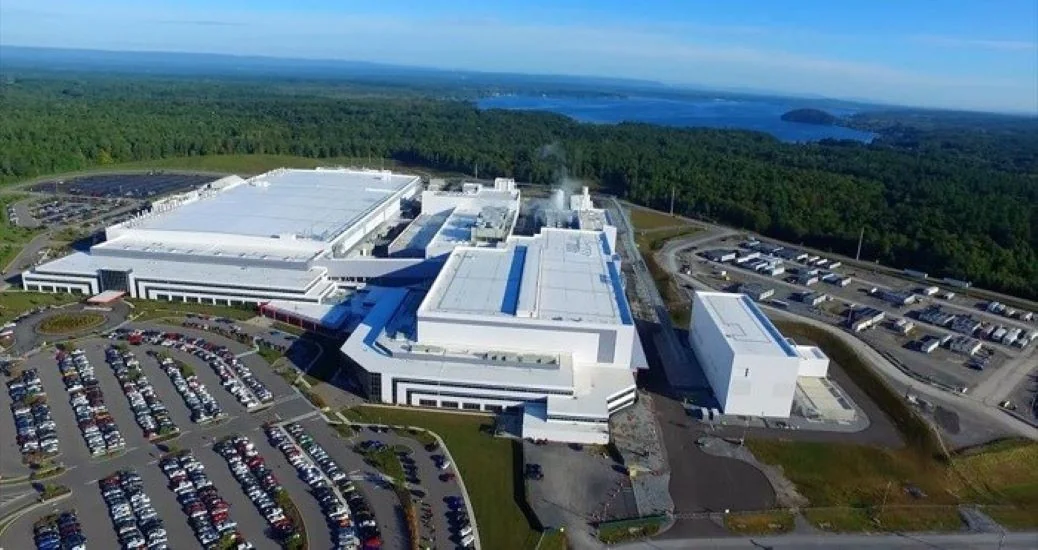
GF's GaN story originates at its historic Fab 9 in Vermont. An industrial landmark since 1957 and a DoD "Trusted Foundry," this 200mm facility provided the perfect launchpad.

The journey began in earnest around 2019, driven by the DoD's Trusted Access Program Office (TAPO). With the goal of establishing a domestic platform for high-frequency, high-power GaN-on-Si applications, TAPO provided $40 million in phased funding from 2020 to 2022. This initial support was crucial for laying the technical groundwork for GF's entry into the defense and communications markets, centered on a 200mm GaN-on-Si process compatible with its existing 180nm CMOS lines.

■ Building an Ecosystem: From Process to Platform Solutions

Recommended by LinkedIn

GF's ambition extends far beyond simple wafer manufacturing. It is building a complete solutions ecosystem integrating process, IP, and advanced packaging. The flagship initiative is its GaN2BCD™ heterogeneous integration technology. By bonding GaN power dies directly to BCD control wafers, this approach promises to dramatically reduce parasitics, shrink form factors, and boost system-level efficiency and reliability.

GF has validated this platform through compelling demonstrations:

Boost Converter: Achieved a 4x increase in load capacity and a 10% boost in peak efficiency.

Class D Audio Amplifier: Reached 91.6% efficiency in a millimeter-scale package.

LED Flash Driver: An integrated GaN LED and CMOS controller eliminated wire bonds, enhancing stability and performance.

To accelerate commercialization, GF has aggressively built out its IP portfolio through:

Acquisition: The 2024 purchase of Tagore Technology's high-power GaN IP portfolio, securing proven 650V E-mode GaN HEMT designs.

Partnership: A collaboration with Finwave Semiconductor to develop a low-voltage, high-gain GaN platform targeting 5G/6G and mobile RF, with mass production slated for early 2026.

By mid-2025, GF's Vermont facility has solidified a comprehensive GaN platform spanning RF and power applications, supported by a full suite of manufacturing and packaging solutions.

🔷 Chapter 3: GF's Technology Playbook – A Strategy of Integration

GF's GaN strategy is a masterclass in leveraging existing strengths to attack new markets. It is a differentiated approach built on a deep understanding of material physics, process integration, and the industry's evolution toward system-level solutions.

■ The Foundation: Why Wide-Bandgap Materials?

The decision to enter GaN is rooted in fundamental physics. With its wide bandgap (3.42 eV), high electron velocity, and low on-resistance, GaN vastly outperforms traditional silicon in high-voltage, high-frequency power applications. Its superior material properties, captured by metrics like the Normalized Johnson FOM (GaN: 28 vs. Si: 1), make it the ideal material for the 50V to 650V range—GF's strategic sweet spot.


Class (B2B/B2C)
B2B
Ingest Status
Rewritten
Dedupe hash
b5af512599445e208de02b48fb4ee39e
Press Eligible
Yes
Press Eligible Reason
Manuelle Prüfung nötig. Risiko: MEDIUM. Flags: ['finance', 'numbers']. Stichprobe: False
Source Name
GlobalFoundries Newsroom
Image URL
https://media.licdn.com/dms/image/v2/D5612AQF71ZLtimR6bA/article-cover_image-shrink_720_1280/B56Zg6b8mMHUAM-/0/1753327069331?e=2147483647&v=beta&t=lDFQBR6WQGi3SvDSodwMgH4Bq5uuntbTie-9A-FsZ34
Content Hash (SHA-256, erste 32 hex)
2b080d90358355fbf3d47e00cefcd962
DoD Partners With GLOBALFOUNDRIES To Manufacture Secure Chips
Image File
Original HTML

DoD Partners With GLOBALFOUNDRIES To Manufacture Secure Chips

The News: In a recently announced strategic partnership, the U.S Department of Defense (DoD) will partner with GLOBALFOUNDRIES, one of the world’s leading specialty foundries, to provide a secure and reliable supply of semiconductor solutions that will be manufactured at Fab 8 in Malta, New York. Read the GLOBALFOUNDRIES press release here.

DoD Partners with GLOBALFOUNDRIES to Manufacture Secure Chips

Analyst Take: The DoD’s partnership with GLOBALFOUNDRIES is both about reliability and security. GLOBALFOUNDRIES’ Fab 8, located in Malta, New York is the company’s most advanced manufacturing facility.

In May of 2020, GLOBALROUNDRIES announced plans to implemented export control security measures, bringing it into compliance with both the U.S. International Traffic in Arms Regulations (ITAR) and the Export Administration Regulations (EAR), making the company the most advanced ITAR foundry in the United States. GLOBALFOUNDRIES has reportedly invested over $13 billion in its Fab 8 facility, and this strategic move is clearly intended to allow the company to serve the U.S. government and meet both its technology and its security needs around semiconductor chips for the foreseeable future.

GLOBALFOUNDRIES Also Pursues Trusted Facility Status from the Pentagon for Fab 8

Following the securing of certification under U.S. export controls to manufacture chips for sensitive military and aerospace applications, GLOBALFOUNDRIES is also currently in talks with the DoD to qualify its Fab 8 facility in New York as a trusted facility. The chipmaker currently has secured trusted facility status for its Fab 9 facility in Burlington, VT and its Fab 10 facility in East Fishkill, NY, with the Vermont foundry being the first facility in the nation to achieve that status back in 2005.

In the interim, as the company pursues trusted facility status for the Fab 8 facility, its ITAR certification allows the foundry to manufacture chips for military and aerospace applications. The DoD is quoted as saying “The agreement with GLOBALFOUNDRIES is just one step the Department of Defense is taking to ensure the U.S. sustains the microelectronics manufacturing capability necessary for national and economic security. This is a pre-cursor to major efforts contemplated by the recently passed CHIPS for America Act, championed by Senator Charles Shumer (D-NY), which will allow for the sustainment and on-shoring of U.S. microelectronics capability.” It should be noted that Schumer tied his support for the CHIPS Act to expanding GLOBALFOUNDRIES’ role as the Pentagon’s primary secure foundry. Beyond the fact that manufacturing semiconductor chips domestically is an important goal for the U.S. in general, the fact that two of the foundry’s U.S. locations are based in New York state was likely a ley driver of Schumer’s support. GLOBALFOUNDRIES employs in the neighborhood of 3,000 people at its Fab 8 facility alone and has clearly not hesitated to invest in both gaining the certifications it requires to continue serving the U.S. government, but also providing a source of jobs in the communities where it is located.

A Global Chip Shortage is a Big Challenge — Subsidizing a Homegrown Chip Industry is Important

It is no secret that the semiconductor industry is struggling due to high demand for chips. Chips make our worlds go around, whether we realize it or not, and a global pandemic has contributed to a global chip shortage. Computer chips (semiconductors) are in everything — laptops, TVs, video game systems, devices, cars, doorbells, and thermostats and more. Chips also power all things related to smart cities and buildings, including but definitely not limited to utilities, power lines, water treatment plants, buildings — you name it, if it’s connected, it’s powered by a semiconductor chip. Not only have we had a global pandemic that has created a surge of demand for consumer devices, we’ve had a trade war with China that has strained chip production.

That’s why efforts to subsidize a homegrown chip industry and reducing the U.S.’s reliance on overseas manufacturers have shifted into high gear. The DoD’s partnership with GLOBALFOUNDRIES comes at a much-needed time. The company’s ITAR certification, it’s continued willingness to invest in facilities and compliance, and its pursuit of trusted facility status all bode well for the future and the ability of the DoD to get the secure chips it needs. I predict we’ll see that trusted facility status happening sooner rather than later and expect good things ahead out of this strategic partnership.

Futurum Research provides industry research and analysis. These columns are for educational purposes only and should not be considered in any way investment advice.

Other insights from Futurum Research:

My colleague Olivier Blanchard and I tackled the topic of the global chip shortage in a recent episode of the Futurum Tech Webcast. If this is a topic of interest, you can find that here: From Mobile Devices to the Automotive Industry, Chips Play an Outsized Role — and a Global Chip Shortage is a Very Big Deal

Here’s What’s in Store for Marvell Technology, Qualcomm, and Other Semiconductor Companies This Year

The original version of this article was first published on Futurum Research.

Class (B2B/B2C)
B2B
Ingest Status
Rewritten
Dedupe hash
ec45e4b4a76d15c79bd53e2d1595d517
Press Eligible
Yes
Press Eligible Reason
Manuelle Prüfung nötig. Risiko: MEDIUM. Flags: ['finance']. Stichprobe: False
Source Name
GlobalFoundries Newsroom
Image URL
https://media.licdn.com/dms/image/v2/C4D12AQGFj8PfqWYkfg/article-cover_image-shrink_600_2000/article-cover_image-shrink_600_2000/0/1614959715328?e=2147483647&v=beta&t=-SkT9Cl3QSzWKph6uRM1jFafNBMKthlUDZD0uwwcp08
Content Hash (SHA-256, erste 32 hex)
add35e2776cbda8acb959c24f1a7e225
Stakeholder Announcements
Original HTML

Stakeholder Announcements

-

Update: OBSI 2026 External Review Public Consultation As previously announced, CRKhoury (CRK) is currently leading an independent review of OBSI’s banking and securities mandates and our overall operations and practices. CRK have established a Review website at obsireview.crkhoury.com.au which provides some information about the Review and will be updated from time to time as the Review progresses.

-

OBSI 2026 External Review Public Consultation As previously announced, CRKhoury (CRK) is currently leading an independent review of OBSI’s banking and securities mandates and our overall operations and practices. The independent review is expected to conclude with the final report published later this year on OBSI’s website.

-

CRKhoury to conduct OBSI’s 2026 independent external reviews OBSI is pleased to announce the appointment of CRKhoury (CRK) to conduct the 2026 independent external review of OBSI’s operations and practices for both banking and investment-related complaints. The purpose of this independent review is to evaluate whether OBSI has fulfilled its regulatory obligations and operates effectively in accordance with recognized best practices for financial services ombudsmen.

-

OBSI hosts annual meeting of financial services ombuds from around the world OBSI is honoured to host financial services ombudsmen from around the world at the 2024 annual conference of the International Network of Financial Services Ombudsman Schemes (INFO Network), which is taking place in Toronto from September 29 to October 2, 2024.

-

OBSI consultation on loss calculation for complaints involving unsuitably sold illiquid exempt market securities – request for public comment September 26, 2024 – The Ombudsman for Banking Services and Investments (OBSI) is now seeking input from stakeholders and the public in relation to our approach to calculating investor losses in cases involving unsuitable sales of illiquid exempt market securities. This consultation is focused on assessing the process we currently use and helping us determine whether there are better alternative approaches we should adopt in such cases. This consultation was recommended in our 2021 independent expert external review. OBSI remains committed to improving its approaches and practices wherever possible.

-

OBSI launches new website We are pleased to announce the launch of our refreshed website. This update brings a contemporary design and user experience to OBSI.ca, making it easier and more intuitive for consumers and firms to access the information and tools they need.

-

OBSI announces search for two new board members We will soon be launching a search for two qualified professionals to join our Board of Directors to fill one current and one expected vacancy. The positions to be filled are for one Industry Director and one Consumer Interest Director. To ensure an open search process and that we are able to identify the best candidates, as part of our search process, we will engage with industry associations and consumer advocacy groups for potential candidate recommendations.

-

OBSI Governance Review – request for public comment November 1, 2022 - As first announced on August 25, the Ombudsman for Banking Services and Investments (OBSI) is now seeking input from stakeholders and the public in relation to its organizational governance. This consultation is focussed on understanding how OBSI’s board can best ensure that it has the opportunity to consider the perspectives of stakeholders with financial service industry expertise and consumer advocacy expertise in its decision making. OBSI is committed to ensuring a deep knowledge of these perspectives at the board level because they are crucial to ensuring that the organization is able to continue to fulfil its mission of helping to ensure a fair, effective and trusted financial services sector. OBSI’s last public consultation on governance reform took place in 2012.

-

OBSI Response to the 2021 Independent Evaluation Recommendations October 26, 2022 - Today, OBSI provided its response to the recommendations included in the 2021 independent evaluations of its investment and banking mandates.

-

OBSI board announces launch of strategic governance review August 25, 2022 - The Board of Directors for the Ombudsman for Banking Services and Investments (OBSI) announced that it has begun a strategic review of its governance structure with plans for public consultation in the late fall.

Class (B2B/B2C)
B2B
Ingest Status
Rewritten
Dedupe hash
827f7dacd8c5b64b29f158f9fd7f63b9
Press Eligible
Yes
Press Eligible Reason
Financial services ombudsman updates on governance, consultations, and independent reviews.
Source Name
Ombudsman for Banking Services and Investments (OBSI)
Image URL
https://media-001-ca.cdn.govstack.com/obsi-006-ca/media/1byowuih/obsi-logo-cropped.svg
Content Hash (SHA-256, erste 32 hex)
f6b829e74273d8cd0dde2f9214ee6f05
MODE Global News
Image File
Original HTML

MODE Global Announces Strategic Partnership with Sync Logistics Training

DALLAS, TEXAS (April 16, 2024) – MODE Global (“MODE”), an industry-leading third-party logistics (3PL) firm is excited to announce a strategic partnership with Sync Logistics Training (“Sync”), an online learning and development platform designed specifically for the transportation industry. The collaboration strengthens MODE’s existing training process and equips employees to deliver the high level of service MODE customers demand.

As the logistics industry continues to evolve, MODE recognizes the critical role training plays in employee success and professional development. By partnering with Sync, MODE can help its employees excel by providing a comprehensive training program tailored to the unique demands of its business model and growth strategy.

“As a participant of the Sync pilot program, when I saw how comprehensive the curriculum and training program was, I knew I wanted to advocate for this tool not only for my team’s development but also as part of an enterprise-wide solution,” said Rob Jernigan, vice president of agent experience at MODE Global. “With the Sync platform, industry knowledge is no longer a stumbling block to employee success.”

Key goals of the partnership include:

- Decrease ramp times and set MODE employees up for long-term success with Sync’s best-in-class industry-specific training.

- Increase MODE employees’ skills and confidence to navigate the complex world of freight brokerage through Sync’s interactive simulations.

- Support MODE’s ongoing investment in employees by providing continuous education and upskilling opportunities.

“Our goal is to help brokers train and retain more proactive and engaged employees,” said Nick Dangles, co-founder of Sync Logistics Training. “We are thrilled to partner with MODE to enhance its employee development initiatives!”

The partnership between MODE and Sync represents a shared commitment to investing in employee development for all MODE employees and to raising the bar of service excellence within the transportation industry.

About Sync Logistics Training

Sync Logistics Training is an online training and development platform, built specifically for the transportation industry. We allow your brokerage to transfer years of industry knowledge to your new employees in an engaging and effective way. Using a mix of video courses, simulations and quizzes, your new hires will reach new heights faster.

Ingest Status
Rejected
Dedupe hash
42ace0831c68d4ba706e89f182199b59
Source Name
MODE Global
Image URL
https://www.modeglobal.com/wp-content/uploads/2024/04/MODE-Global-Sync-News-Page-Image-.png
Source Node
Content Hash (SHA-256, erste 32 hex)
6ddf67d29ad627a58aa3eb6abe8e6cce
CMS outlines comprehensive strategy to foster innovation for transformative medical technologies
Original HTML

CMS outlines comprehensive strategy to foster innovation for transformative medical technologies

Today at the Medical Device Manufacturers Association (MDMA) Annual Meeting, Centers for Medicare & Medicaid Services (CMS) Administrator Seema Verma for the first time walked through the agency’s comprehensive strategy to improve patients’ access to emerging technologies. The future directions outlined in today’s address build on recently released CMS policies to unleash innovation in our healthcare system, reinforcing the Trump Administration’s commitment to encouraging a competitive market that lowers cost and increases the quality of and access to healthcare for all Americans.

“Innovation is the fuel that powers the engine of progress and creativity. That is why the Trump Administration is taking action in every possible way to promote, enhance, and foster innovation within the healthcare system,” said CMS Administrator Seema Verma. “We are committed to removing government barriers and modernizing regulations around new technologies to ensure safe and effective treatments are readily accessible to beneficiaries without delaying patient care.”

The Administrator highlighted two specific actions in today’s address.

First, for issuing Healthcare Common Procedure Coding System (HCPCS) codes, CMS is changing the current process of allowing only one opportunity per year to apply for new Level II codes. The agency is moving to a process with quarterly opportunities to apply for drugs, and semi-annual opportunities to apply for devices. CMS anticipates this will greatly improve the ability for technologies to move through the adoption curve, and additional details will be forthcoming on the updates to the process.

Second, for technologies with Current Procedural Terminology (CPT) Category III codes (which are temporary codes used for emerging technologies), CMS is clarifying that for technologies that do not fall under an existing LCD, Medicare contractors are required to follow the transparent new Local Coverage Determination process for every local coverage decision, including reviewing the evidence with respect to the technology. This clarification was part of a list of answers to commonly asked questions about the Local Coverage Determination process that the agency posted online earlier today.

Taken together with other CMS actions, these two actions represent key components of a comprehensive CMS strategy to address barriers to medical innovation in the Medicare program. Just last week in the Inpatient Prospective Payment System (IPPS) proposed rule, CMS proposed a number of changes to advance innovation, including proposing to increase the new technology add-on payment which provides hospitals with additional payments for cases with high costs involving new technology. CMS also proposed to modernize payment policies for medical devices that meet FDA’s Breakthrough Devices designation. The agency’s strategy overall will help ensure predictable coverage pathways, enhance opportunities for coverage for transformative technologies, reduce wait times to apply for permanent codes, and modernize payment for innovative services.

Administrator Verma’s speech can be viewed at: https://www.cms.gov/newsroom/press-releases/speech-remarks-administrator-seema-verma-medical-device-manufacturers-association.

###

Get CMS news at cms.gov/newsroom, sign up for CMS news via email and follow CMS @CMSgov

Class (B2B/B2C)
B2B
Ingest Status
Rewritten
Dedupe hash
f21e8ca5f5369d04b0401de62e392f15
Press Eligible
Yes
Press Eligible Reason
CMS policy update on coding, coverage, and payments for emerging medical technologies, relevant to healthcare and device industry professionals.
Source Name
AdvaMed News
Source Node
Content Hash (SHA-256, erste 32 hex)
bb0bfca7181ad16382289548cd0fc41f