By Editor , 14 September 2026
DJI Hosts Filmmaker Forum in Venice to Showcase Osmo Pocket 4P

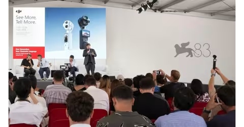
Venice – September 13, 2026 -- DJI staged a professional forum titled the "Filmmakers & Visionaries Session" at the Venice Production Bridge during the 83rd Venice International Film Festival, using the event to argue that its pocket-sized Osmo Pocket 4P camera can meet the technical standards of professional cinema.

By Editor , 14 September 2026
La Luce Cristallina Launches STO Wafer Platform for Quantum Devices

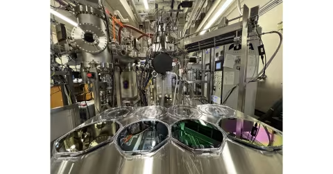
Austin, Texas – – September 13, 2026 -- La Luce Cristallina has launched a 0.5-micrometer silicon-based quantum paraelectric strontium titanate on insulator (QP-STOI) wafer platform, giving researchers and national laboratories a new tool for building next-generation cryogenic and quantum devices.

By Editor , 13 September 2026
Ceva, LG Electronics Combine UWB Tech, Land Major US Chipmaker Client

Rockville, Md. and Seoul, South Korea – September 13, 2026 -- Ceva, Inc. (NASDAQ: CEVA) and LG Electronics have secured a major U.S. semiconductor company as a customer for a jointly developed Ultra-Wideband (UWB) solution, marking commercial validation for the two-company collaboration announced today.

By Editor , 13 September 2026
SK keyfoundry Locks Elmos Into Wafer Supply Deal Through 2037

Seoul – September 13, 2026 -- SK keyfoundry has signed a long-term wafer supply agreement with Elmos Semiconductor SE that guarantees production capacity through 2037, extending an 18-year partnership between the Korean 8-inch foundry and the German automotive chipmaker.

The deal, signed during a ceremony in Frankfurt am Main, shifts the two companies' collaboration from 350nm to 130nm process technology, marking the first major node transition in nearly two decades of cooperation.

By Editor , 13 September 2026
DB HiTek Completes 8-Inch 1,200V SiC MOSFET Reliability Qualification

Seoul – September 12, 2026 -- DB HiTek has completed reliability qualification for its 1,200 V silicon carbide (SiC) MOSFET process on 8-inch (200 mm) wafers, establishing what it calls the world's first complete 8-inch SiC foundry process flow. The South Korean pure-play foundry targets volume production in 2027.

By Editor , 13 September 2026
DB HiTek Completes World-First 8-Inch SiC MOSFET Qualification

Seoul – September 12, 2026 -- DB HiTek has completed reliability qualification for its 8-inch (200mm) 1,200V silicon carbide (SiC) MOSFET manufacturing process, establishing what the company calls the world's first complete foundry production flow for 8-inch SiC power semiconductors. Mass production is targeted for 2027.

By Editor , 13 September 2026
DB HiTek Completes Reliability Qualification for 8-Inch 1,200V SiC MOSFET Process

Seoul – September 12, 2026 -- DB HiTek has completed reliability qualification for its 1,200V silicon carbide (SiC) MOSFET manufacturing process on 8-inch (200mm) wafers, establishing what the company calls the world's first complete 8-inch SiC foundry process. Mass production is scheduled for 2027.

By Editor , 13 September 2026
DB HiTek Clears Reliability Tests for 1,200V SiC MOSFETs on 8-Inch Wafers

Seoul – September 12, 2026 -- DB HiTek has completed reliability qualification testing for its 1,200V silicon carbide (SiC) MOSFET process on 8-inch (200mm) wafers, establishing what the company calls the world's first full-service process for 8-inch SiC semiconductor production.

By Editor , 13 September 2026
DB HiTek Completes Reliability Qualification for 8-Inch SiC MOSFET Process

Seoul – September 12, 2026 -- DB HiTek has completed reliability qualification for its 1,200-V silicon carbide (SiC) MOSFET process on 8-inch (200mm) wafers, establishing what the company calls the world's first complete 8-inch SiC foundry process flow. The South Korean pure-play foundry targets mass production in 2027.

By Editor , 13 September 2026
DB HiTek Completes Reliability Qualification for 8-Inch SiC MOSFET Process

Seoul – September 12, 2026 -- DB HiTek has completed reliability qualification for its 1,200V silicon carbide (SiC) MOSFET process on 8-inch (200mm) wafers, establishing what the company calls the world's first complete 8-inch SiC foundry process flow. The South Korean foundry, which specializes in 8-inch wafer production, is targeting volume manufacturing of the technology in 2027.