DB HiTek прошла квалификационные испытания на надежность для процесса SIC MOSFET на 1 200 В
Image File
Original HTML

DB HiTek прошла квалификационные испытания на надежность для процесса SIC MOSFET на 1 200 В

- Компания создает первый в мире полнофункциональный технологический процесс для производства 8-дюймовых пластин из карбида кремния

- Комплекты проектирования для разработки микросхем (PDK) первого и второго поколения доступны для клиентов, а выпуск PDK третьего поколения запланирован на ноябрь. Ожидается, что время разработки продукта сократится более чем на один год

СЕУЛ, Южная Корея, 9 сентября 2026 г. /PRNewswire/ -- Компания DB HiTek, ведущий южнокорейский специализированный производитель микросхем на 8-дюймовых пластинах, объявила об успешном завершении квалификационных испытаний на надежность для процесса изготовления кремний-карбидных (SiC) МОП-транзисторов (MOSFET) на 1 200 В на 8-дюймовых (200 мм) пластинах. Это достижение знаменует собой новый шаг в экспансии компании на рынок 8-дюймовых кремний-карбидных полупроводников с плановым объемом производства на 2027 год. С учетом пройденных квалификационных испытаний DB HiTek планирует усилить поддержку разработки продуктов для клиентов, найти новых клиентов и ускорить подготовку к серийному производству в 2027 году.

Карбид кремния (SiC) — это прочный материал для полупроводников следующего поколения, который обладает улучшенными характеристиками по сравнению с обычным кремнием (Si) в высокотемпературных и высоковольтных средах, что делает его пригодным для использования в электромобилях (EV), системах возобновляемых источников энергии и промышленного энергетического оборудования. В то время как 6-дюймовые пластины в настоящее время доминируют на рынке карбида кремния, крупные мировые производители полупроводников переходят на 8-дюймовые пластины для повышения эффективности производства и конкурентоспособной стоимости. DB HiTek отреагировала на этот рыночный переход разработкой технологии процесса производства 8-дюймовых пластин из карбида кремния и созданием собственных полупроводниковых сервисов.

Благодаря оптимизации процесса производства МОП-транзисторов из карбида кремния компания DB HiTek достигла конкурентоспособных электрических характеристик и высокого уровня надежности. Компания наладила первый в мире полнофункциональный технологический процесс производства 8-дюймовых карбид-кремниевых пластин на 1 200 В, создав сервисную платформу для производства полупроводников, способную поддерживать клиентов при проектировании, производстве, определении электрических характеристик и квалификации надежности.

Чтобы поддержать коммерческое развертывание своего бизнеса по производству 8-дюймовых кремний-карбидных пластин, DB HiTek предоставляет клиентам комплекты проектирования для разработки микросхем (PDK) для своих запатентованных процессов производства МОП-транзисторов первого и второго поколения на 1 200 В. Третье поколение PDK планируется выпустить в ноябре этого года. Используя эти PDK, клиенты могут сократить ресурсы, необходимые на начальных этапах разработки, ускорить изготовление прототипов и сократить время разработки продукта более чем на один год.

Процесс второго поколения, охватываемый PDK, достигает удельного сопротивления (Rsp) 2,5 мОм/см² или менее и порогового напряжения (Vth) 3 В или выше при напряжении на затворе в открытом состоянии (Vgs(on)) 18 В. Он также прошел квалификационные испытания на надежность, что является сложной стадией разработки процесса.

Процесс третьего поколения, запланированный к выпуску в ноябре этого года, проходит сейчас квалификационные испытания с целью достижения удельного сопротивления 2,3 мОм/см² или менее при одинаковом напряжении на затворе в открытом состоянии 18 В вместе со временем безопасного воздействия короткого замыкания (SCWT) не менее 2,5 мкс в области безопасной работы при коротком замыкании (SCSOA). После завершения квалификационных испытаний DB HiTek планирует сделать PDK третьего поколения доступным для клиентов.

DB HiTek планирует завершить подготовку процесса и обеспечить доступ к нему постоянным клиентам в третьем квартале этого года. Компания планирует сделать услугу доступной для всех клиентов, начиная со второго квартала 2027 года.

«Завершение квалификационных испытаний на надежность для нашего процесса производства кремний-карбидных МОП-транзисторов на 1 200 В имеет важное значение, поскольку оно демонстрирует, что мы обеспечили основную технологическую и производственную основу, необходимую для предоставления первого в мире сервиса для кремний-карбидных полупроводников на 8-дюймовых пластинах», — сказал представитель DB HiTek. «Мы продолжим подготовку к серийному производству 8-дюймовых кремний-карбидных пластин в 2027 году с целью определения позиции компании на рынке и укрепления нашей конкурентоспособности в секторе производства силовых полупроводников следующего поколения».

Share this article
Class (B2B/B2C)
B2B
Ingest Status
Rewritten
Dedupe hash
0f1e2675196bfc5b8f956d3732108c01
Press Eligible
Yes
Press Eligible Reason
Корпоративная новость о квалификации технологии SiC MOSFET, производстве 8-дюймовых полупроводниковых пластин и коммерческих PDK для клиентов.
Source Name
Unknown Company
Original Summary

<p>Компания создает первый в мире полнофункциональный технологический процесс для производства 8-дюймовых пластин из карбида кремния Комплекты проектирования для разработки микросхем (PDK) первого и второго поколения доступны для клиентов, а выпуск PDK третьего поколения запланирован на...</p>

Image URL
https://mmx.prnewswire.com/media/MS1663041/image-5026888-21003402-Logo.jpg?id=OA2933013&p=facebook
EZVIZ ushers in an era of smart convenience with its scenario-based smart entry portfolio, spanning innovative video doorbells, video doorphones, and gate openers
Image File
Original HTML

EZVIZ ushers in an era of smart convenience with its scenario-based smart entry portfolio, spanning innovative video doorbells, video doorphones, and gate openers

HOOFDDORP, Netherlands, Sept. 9, 2026 /PRNewswire/ -- As innovation showcases at IFA grow increasingly fierce, EZVIZ elevates the conversation with AI-powered technology and extensive product lineups designed for European families at Hall 1.2. Prioritizing users' needs, the company draws attention back on intuitive engagement and easy adoption, exemplified by its award-winning smart entry solutions for smart home convenience.

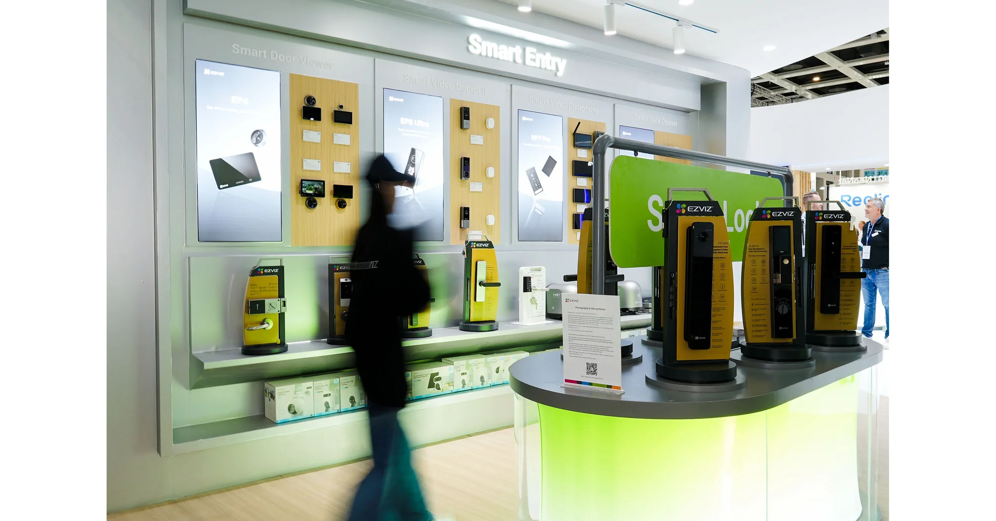
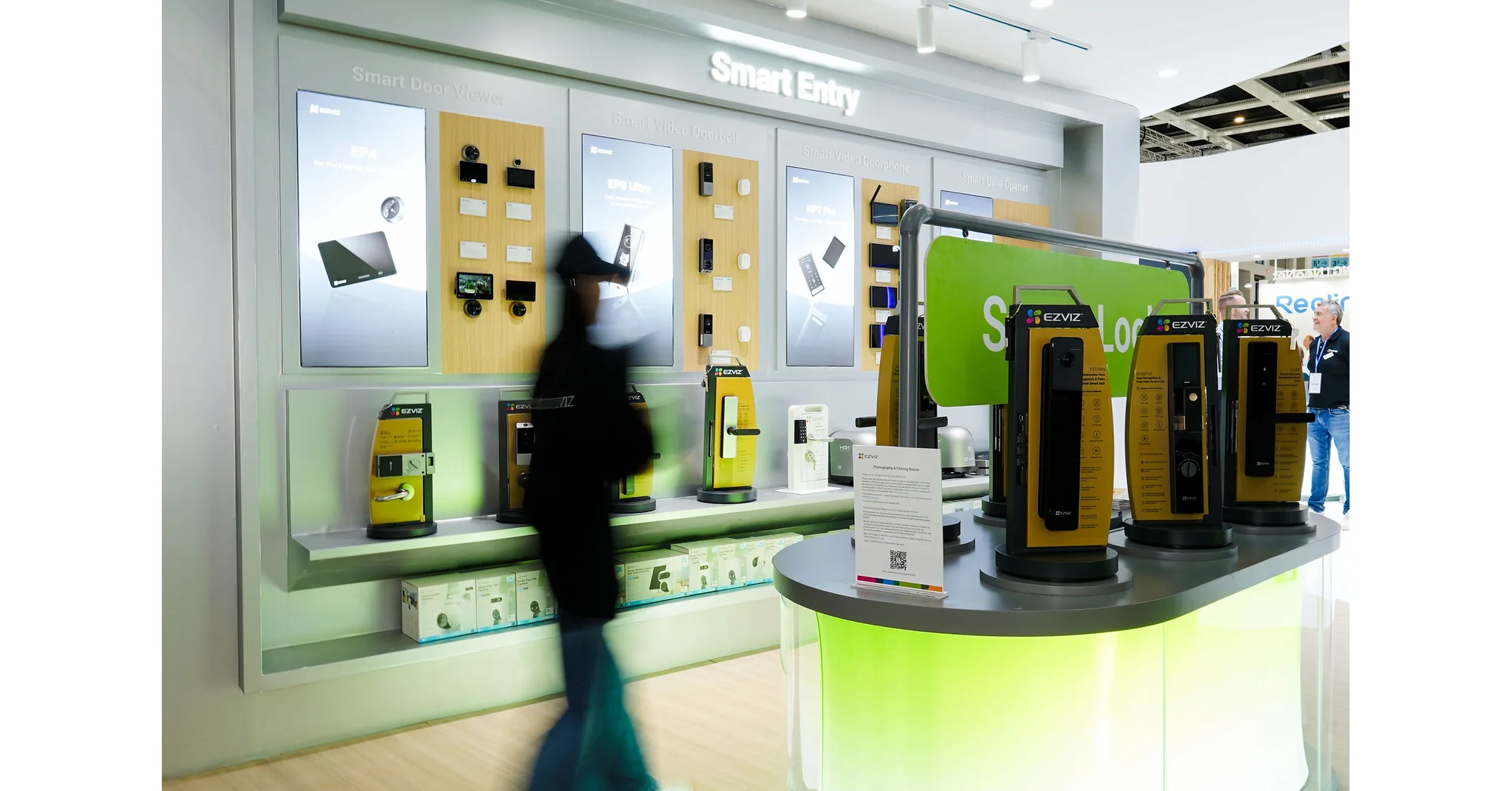
Extending its visual expertise and design philosophy across its wide collection of home access products, EZVIZ has refreshed the market with AI-powered video doorbells, video doorphones, and gate openers that address niche demands in entrance interaction. Further refining real-life scenarios, EZVIZ taps into users' deeply rooted needs and has created probably the most versatile smart entry lineup in the industry, tailored to European lifestyles regardless of family size or accommodation type. With international recognition for its flagship models and brand impact, EZVIZ has once again won the Digital Trends Publisher Awards for its smart entry family at IFA.

"We want our home technology offerings to go beyond smart cameras and extend to entry and daily convenience," said Jasmine Zhu, Product Manager of EZVIZ Europe. "With EZVIZ smart entry devices, we want European users to easily find the perfect match and enjoy true convenience from the very first moment they enter their homes."

The EP8 Ultra video doorbell continues to shine following the popularity of its launch just before IFA, thanks to its built-in AI screen. It's a powerful combination of advanced AI and pioneering design that targets specific entrances like apartment hallways, according to Zhu. Upgraded from dual-lens video doorbells that can see visitors and packages – still a rare innovation among current options – the EP8 Ultra features an interactive screen with AI characters for emotional connection, and on-device AI recognition of familiar faces for energy-saving understanding, making the entrance more connected and cared for than ever.

Beyond single-touchpoint options, EZVIZ also presents systematic solutions – video doorphones and gate openers – and excites audiences by spoiling upcoming models. Building on the success of the HP7 and HP7 Pro video doorphones, the HP7 Battery makes wireless connection a reality, freeing users from wiring and manual maintenance by powering itself with a battery and solar charging. It wipes out remaining concerns about embracing seamless unlocking and remote access management that might arise from complicated installation.

What's more, EZVIZ completes its systematic solutions for houses with driveways with the new HG1 250 Pro for arm-swing gates and the new HG3 300 Pro for cylinder-swing gates. Together with the HG2 600 Pro sliding gate openers, this lineup covers virtually all gate types with different weights and opening methods found in Europe, lowering the barriers to DIY-friendly smart access for more households.

Beyond smart entry, EZVIZ delivers an immersive experience of a futuristic smart home across its five product areas on site. For more information, visit EZVIZ's online booth.

Share this article

Class (B2B/B2C)
B2C
Ingest Status
Rewritten
Dedupe hash
25c438eeca18feeb7e7ff9a34d5034dd
Press Eligible
Yes
Press Eligible Reason
EZVIZ is launching AI-powered smart home entry products, including video doorbells, doorphones, and gate openers, for household consumers.
Source Name
Unknown Company
Original Summary

<p>HOOFDDORP, Netherlands, Sept. 9, 2026 /PRNewswire/ -- As innovation showcases at IFA grow increasingly fierce, EZVIZ elevates the conversation with AI-powered technology and extensive product lineups designed for European families at Hall 1.2. Prioritizing users' needs, the company draws...</p>

Image URL
https://mmx.prnewswire.com/media/MS1983401/EZVIZ-Smart-Entry-Highlights-PR-Picture.jpg?id=OA2935124&p=facebook
DB HiTek schließt die Zuverlässigkeitsqualifizierung für den 8-Zoll-1.200-V-SiC-MOSFET-Prozess ab
Image File
Original HTML

DB HiTek schließt die Zuverlässigkeitsqualifizierung für den 8-Zoll-1.200-V-SiC-MOSFET-Prozess ab

- Etabliert den weltweit ersten vollständigen 8-Zoll-SiC-Foundry-Prozessablauf

- Stellt Kunden PDKs der ersten und zweiten Generation zur Verfügung; PDK der dritten Generation ist für November geplant; erwartet wird eine Verkürzung der Produktentwicklungszeit um mehr als ein Jahr

SEOUL, Südkorea, 9. September 2026 /PRNewswire/ -- DB HiTek, Südkoreas führende reine 8-Zoll-Foundry, gab bekannt, dass sie die Zuverlässigkeitsqualifizierung für ihren 1.200-V-Siliziumkarbid (SiC)-MOSFET-Prozess auf 8-Zoll-Wafern (200 mm) erfolgreich abgeschlossen hat. Dieser Erfolg markiert einen Meilenstein bei der Expansion des Unternehmens in den Markt für 8-Zoll-SiC-Foundry-Dienstleistungen, wobei die Serienproduktion für 2027 angestrebt wird. Aufbauend auf dem Abschluss dieser Qualifizierung plant DB HiTek, die Unterstützung bei der Produktentwicklung für Kunden zu verstärken, neue Kunden zu gewinnen und die Vorbereitungen für die Serienproduktion im Jahr 2027 zu beschleunigen.

Siliziumkarbid (SiC) ist ein Leistungshalbleitermaterial der nächsten Generation, das in Hochtemperatur- und Hochspannungsumgebungen eine überlegene Leistung gegenüber herkömmlichem Silizium (Si) bietet und sich daher besonders gut für Elektrofahrzeuge (EVs), Anlagen für erneuerbare Energien und industrielle Leistungselektronik eignet. Während derzeit 6-Zoll-Wafer den SiC-Markt dominieren, stellen große globale Halbleiterhersteller auf 8-Zoll-Wafer um, um die Produktionseffizienz und die Kostenwettbewerbsfähigkeit zu verbessern. DB HiTek hat auf diesen Marktwandel reagiert, indem das Unternehmen eine 8-Zoll-SiC-Prozesstechnologie entwickelt und seine Foundry-Dienstleistungskapazitäten ausgebaut hat.

Durch die Optimierung seines Hochleistungs-SiC-MOSFET-Prozesses hat DB HiTek wettbewerbsfähige elektrische Eigenschaften und ein hohes Maß an Zuverlässigkeit erreicht. Das Unternehmen hat den weltweit ersten vollständigen 1.200-V-8-Zoll-SiC-Foundry-Prozessablauf etabliert und damit eine Foundry-Service-Plattform geschaffen, die Kunden in den Bereichen Design, Fertigung, elektrische Charakterisierung und Zuverlässigkeitsqualifizierung unterstützt.

Zur Unterstützung der kommerziellen Einführung seines 8-Zoll-SiC-Foundry-Geschäfts stellt DB HiTek seinen Kunden Process Design Kits (PDKs) für seine proprietären 1.200-V-SiC-MOSFET-Prozesse der ersten und zweiten Generation zur Verfügung. Ein PDK der dritten Generation soll im November dieses Jahres herauskommen. Durch den Einsatz dieser PDKs können Kunden den Ressourcenbedarf in den Anfangsphasen der Entwicklung reduzieren, die Prototypenfertigung beschleunigen und die Produktentwicklungszeit um mehr als ein Jahr verkürzen.

Der im PDK enthaltene Prozess der zweiten Generation erreicht einen spezifischen Ein-Widerstand (Rsp) von 2,5 mΩ •cm² oder weniger und eine Schwellenspannung (Vth) von 3 V oder mehr bei einer Gate-Spannung im eingeschalteten Zustand (Vgs(on)) von 18 V. Zudem hat er die Zuverlässigkeitsqualifizierung abgeschlossen, eine anspruchsvolle Phase der Prozessentwicklung.

Der Prozess der dritten Generation, dessen Veröffentlichung für November geplant ist, wird derzeit qualifiziert, mit dem Ziel, einen spezifischen Durchlasswiderstand von 2,3 mΩ •cm² oder weniger bei derselben Gate-Spannung im eingeschalteten Zustand von 18 V zu erreichen, zusammen mit einer Kurzschluss-Festigkeitsdauer (SCWT) von mindestens 2,5 μs im kurzschlusssicheren Betriebsbereich (SCSOA). Sobald die Qualifizierung abgeschlossen ist, plant DB HiTek, das PDK der dritten Generation den Kunden zur Verfügung zu stellen.

DB HiTek plant, die Prozessvorbereitungen im dritten Quartal dieses Jahres abzuschließen und langjährigen Kunden Zugang zu gewähren. Das Unternehmen plant, den Dienst ab dem zweiten Quartal 2027 allen Kunden zur Verfügung zu stellen.

„Der Abschluss der Zuverlässigkeitsqualifizierung für unseren 1.200-V-SiC-MOSFET-Prozess ist von großer Bedeutung, da er zeigt, dass wir die Kernprozesstechnologie und die Fertigungsgrundlage gesichert haben, die erforderlich sind, um den weltweit ersten 8-Zoll-SiC-Foundry-Service anzubieten", sagte ein Vertreter von DB HiTek. „Wir werden die Vorbereitungen für die Serienproduktion von 8-Zoll-SiC 2027 fortsetzen, mit dem Ziel, uns auf dem Markt zu etablieren und unsere Wettbewerbsfähigkeit im Bereich der Foundry-Dienstleistungen für Leistungshalbleiter der nächsten Generation zu stärken."

Share this article

Class (B2B/B2C)
B2B
Ingest Status
Rewritten
Dedupe hash
6cf72634da012696c55fe23d310a402d
Press Eligible
Yes
Press Eligible Reason
Unternehmensnachricht über DB HiTeks 8-Zoll-SiC-Foundry, Prozessqualifizierung, PDKs und geplante Serienproduktion für Kunden und Industriepartner.
Source Name
Unknown Company
Original Summary

<p>Etabliert den weltweit ersten vollständigen 8-Zoll-SiC-Foundry-Prozessablauf Stellt Kunden PDKs der ersten und zweiten Generation zur Verfügung; PDK der dritten Generation ist für November geplant; erwartet wird eine Verkürzung der Produktentwicklungszeit um mehr als ein Jahr SEOUL,...</p>

Image URL
https://mmx.prnewswire.com/media/MS1663041/image-5026888-21003402-Logo.jpg?id=OA2933011&p=facebook
Flytxt's Agentic AI Niya-X Wins Bronze Stevie® at the 2026 International Business Awards®
Image File
Original HTML

Flytxt's Agentic AI Niya-X Wins Bronze Stevie® at the 2026 International Business Awards®

DUBAI, UAE, Sept. 9, 2026 /PRNewswire/ -- Flytxt today announced that its Agentic AI platform, Niya-X, has won a Bronze Stevie® Award in the 'Best AI-driven Product' category at the 23rd Annual International Business Awards® (IBAs).

Niya-X introduces an AI Expertforce for enterprises - moving beyond AI Co-pilots that assist people and task-oriented AI agents that automate work. Its domain-specific AI Experts can understand business goals, formulate strategies, make decisions, orchestrate actions and continuously learn from outcomes. Powered by causal learning and counterfactual modeling, Niya-X can simulate and evaluate alternate scenarios in given marketplace setting before determining the course of action most likely to achieve a desired outcome, while operating within defined enterprise guardrails and privacy requirements.

"This award reinforces the transformative potential of Niya-X and its broader applicability in enabling more autonomous enterprise marketplaces," said Dr. Vinod Vasudevan, CEO, Flytxt. "By moving AI from automating tasks and augmenting human intelligence to actively shaping strategic decisions and actions, Niya-X enables enterprises to continuously adapt their decisions and drive better outcomes in complex and dynamic business environments."

The International Business Awards are the world's premier business awards program, open to organizations of all sizes and sectors globally. The 2026 IBAs received more than 3,400 nominations from 82 nations and territories. Winners were evaluated by over 200 business professionals serving on specialized judging committees, with final scores determined through an independent judging process in June and July. Stevie Award winners will be celebrated at a gala event at the Pullman Paris Montparnasse on Wednesday, 28 October 2026.

Across enterprise marketplaces, Niya-X AI Experts are being applied to a broad range of use cases spanning customer growth and retention, product design and pricing, as well as employee on-boarding and engagement. Deployments include optimising investment recommendations to grow Assets Under Management (AUM), predicting and acting on customer intent to improve service efficiency, designing and executing on-boarding journeys for new employees and autonomously orchestrating growth marketing decisions and actions.

To know more, please visit www.flytxt.ai

Share this article

Class (B2B/B2C)
B2B
Ingest Status
Rewritten
Dedupe hash
df94e9be3dc03bf2b41ea59a721d2b00
Press Eligible
Yes
Press Eligible Reason
Corporate announcement about an enterprise AI product, its award, capabilities, and business deployments.
Source Name
Unknown Company
Original Summary

<p>DUBAI, UAE, Sept. 9, 2026 /PRNewswire/ -- Flytxt today announced that its Agentic AI platform, Niya-X, has won a Bronze Stevie® Award in the 'Best AI-driven Product' category at the 23rd Annual International Business Awards® (IBAs). Niya-X introduces an AI Expertforce for enterprises -...</p>

Image URL
https://mmx.prnewswire.com/media/MS1983245/Stevie-Awards-Badge.jpg?id=OA2934583&p=facebook
DB HiTek má kvalifikaci spolehlivosti pro osmipalcovou výrobu SiC MOSFETů s napětím 1 200 V
Image File
Original HTML

DB HiTek má kvalifikaci spolehlivosti pro osmipalcovou výrobu SiC MOSFETů s napětím 1 200 V

- Zavádí první kompletní osmipalcový výrobní proces pro SiC (karbid křemíku) na světě

- Zákazníkům poskytuje PDK (sadu pro návrh výrobního procesu) první a druhé generace, PDK třetí generace je naplánována na listopad; očekává se zkrácení doby vývoje produktu o více než jeden rok

SOUL, Jižní Korea, 9. září 2026 /PRNewswire/ -- Společnost DB HiTek, přední jihokorejská specializovaná osmipalcová slévárna, oznámila, že úspěšně dokončila kvalifikaci spolehlivosti svého procesu výroby MOSFETů z karbidu křemíku (SiC) s napětím 1 200 V na osmipalcových (200 mm) destičkách. Tento úspěch představuje významný krok v rámci expanze společnosti na trh osmipalcových SiC sléváren, přičemž zahájení sériové výroby je plánováno na rok 2027. Na základě dokončení této kvalifikace plánuje společnost DB HiTek posílit podporu vývoje produktů pro zákazníky, získat nové zákazníky a urychlit přípravy na sériovou výrobu v roce 2027.

Karbid křemíku je materiál nové generace pro výkonové polovodiče, který v prostředí s vysokými teplotami a vysokým napětím nabízí lepší výkon než konvenční křemík (Si), díky čemuž je velmi vhodný pro elektromobily (EV), systémy využívající obnovitelné zdroje energie a průmyslová energetická zařízení. Ačkoli na trhu se SiC v současné době dominují šestipalcové destičky, přední světoví výrobci polovodičů přecházejí na osmipalcové destičky, aby zvýšili efektivitu výroby a nákladovou konkurenceschopnost. Společnost DB HiTek reagovala na tuto změnu na trhu vývojem technologie výroby osmipalcových SiC destiček a rozvojem svých kapacit v oblasti slévárenských služeb.

Díky optimalizaci svého procesu výroby vysokovýkonných SiC MOSFETů dosáhla společnost DB HiTek konkurenceschopných elektrických charakteristik a vysoké úrovně spolehlivosti. Společnost zavedla první kompletní proces výroby osmipalcových SiC destiček s napětím 1 200 V na světě a vytvořila tak platformu slévárenských služeb schopnou podporovat zákazníky v oblastech návrhu, výroby, elektrické charakterizace a kvalifikace spolehlivosti.

Za účelem podpory komerčního zavádění své činnosti v oblasti výroby osmipalcových SiC čipů poskytuje společnost DB HiTek zákazníkům sady pro návrh procesů (PDK) pro své vlastní procesy výroby SiC MOSFETů první a druhé generace s napětím 1 200 V. Uvedení PDK třetí generace je naplánováno na listopad tohoto roku. Díky těmto sadám PDK mohou zákazníci snížit nároky na zdroje v počátečních fázích vývoje, urychlit výrobu prototypů a zkrátit dobu vývoje produktu o více než jeden rok.

Proces druhé generace, na který se vztahuje sada PDK, dosahuje specifického odporu v zapnutém stavu (Rsp) 2,5 mΩ•cm² nebo méně a prahového napětí (Vth) 3 V nebo více při napětí na hradle v zapnutém stavu (Vgs(on)) 18 V. Prošel také kvalifikací spolehlivosti, což je náročná fáze vývoje procesu.

Proces třetí generace, jehož uvedení na trh je plánováno na listopad, právě prochází kvalifikací s cílem dosáhnout specifického odporu v zapnutém stavu 2,3 mΩ•cm² nebo méně při stejném napětí na hradle v zapnutém stavu 18 V, spolu s dobou odolnosti proti zkratu (SCWT) nejméně 2,5 μs v oblasti bezpečného provozu při zkratu (SCSOA). Jakmile bude kvalifikace dokončena, společnost DB HiTek plánuje zpřístupnit PDK třetí generace zákazníkům.

Společnost DB HiTek plánuje dokončit přípravy výrobního procesu a poskytnout přístup svým dlouhodobým zákazníkům ve třetím čtvrtletí tohoto roku. Od druhého čtvrtletí roku 2027 hodlá společnost tuto službu zpřístupnit všem zákazníkům.

„Dokončení kvalifikace spolehlivosti našeho procesu výroby SiC MOSFETů s napětím 1 200 V je významné, protože dokazuje, že jsme si zajistili klíčovou procesní technologii a výrobní zázemí potřebné k poskytování první osmipalcové SiC slévárenské služby na světě," uvedl zástupce společnosti DB HiTek. „Budeme pokračovat v přípravách na sériovou výrobu osmipalcových SiC v roce 2027 s cílem upevnit si pozici na trhu a posílit naši konkurenceschopnost v odvětví sléváren výkonových polovodičů nové generace."

Share this article

Class (B2B/B2C)
B2B
Ingest Status
Rewritten
Dedupe hash
2ffd081a9b499e6e6c3d3378877a0ce3
Press Eligible
Yes
Press Eligible Reason
QA FAIL (need review): TARGET subheadline claims 'sub-2.5 mΩ·cm2' (less than 2.5), but SOURCE specifies '2.5 mΩ·cm2 or less'. The body is accurate, but the subheadline is a materially stricter claim not supported by the source.
Source Name
Unknown Company
Original Summary

<p>Zavádí první kompletní osmipalcový výrobní proces pro SiC (karbid křemíku) na světě Zákazníkům poskytuje PDK (sadu pro návrh výrobního procesu) první a druhé generace, PDK třetí generace je naplánována na listopad; očekává se zkrácení doby vývoje produktu o více než jeden rok SOUL, Jižní...</p>

Image URL
https://mmx.prnewswire.com/media/MS1663041/image-5026888-21003402-Logo.jpg?id=OA2933008&p=facebook
DB HiTek finaliza la cualificación de fiabilidad para el proceso MOSFET de SiC de 8 pulgadas y 1.200 V
Image File
Original HTML

DB HiTek finaliza la cualificación de fiabilidad para el proceso MOSFET de SiC de 8 pulgadas y 1.200 V

- Establece el primer flujo de proceso completo de fundición de SiC de 8 pulgadas del mundo.

- Proporciona kits de diseño de procesos (PDK) de primera y segunda generación a los clientes, con el PDK de tercera generación programado para noviembre; se espera que reduzca el tiempo de desarrollo del producto en más de un año

SEÚL, Corea del Sur, 9 de septiembre de 2026 /PRNewswire/ -- DB HiTek, la fundición líder en Corea del Sur especializada en obleas de 8 pulgadas, anunció que ha completado con éxito la cualificación de fiabilidad de su proceso MOSFET de carburo de silicio (SiC) de 1.200 V en obleas de 8 pulgadas (200 mm). Este logro representa un paso importante en la expansión de la compañía en el mercado de fundición de SiC de 8 pulgadas, con el objetivo de iniciar la producción en volumen en 2027. Tras completar esta cualificación, DB HiTek planea reforzar el soporte para el desarrollo de productos para sus clientes, captar nuevos clientes y acelerar los preparativos para la producción en volumen en 2027.

El carburo de silicio (SiC) es un material semiconductor de potencia de última generación que ofrece un rendimiento superior al del silicio (Si) convencional en entornos de alta temperatura y alto voltaje, lo que lo hace idóneo para vehículos eléctricos (VE), sistemas de energía renovable y equipos de potencia industrial. Si bien las obleas de 6 pulgadas dominan actualmente el mercado del SiC, los principales fabricantes mundiales de semiconductores están migrando a obleas de 8 pulgadas para mejorar la eficiencia de la producción y la competitividad de costes. DB HiTek ha respondido a esta transición del mercado desarrollando tecnología de proceso para SiC de 8 pulgadas y ampliando sus capacidades de servicio de fundición.

Mediante la optimización de su proceso de MOSFET de SiC de alta potencia, DB HiTek ha logrado características eléctricas competitivas y un alto nivel de fiabilidad. La empresa ha establecido el primer flujo de proceso de fundición completo de SiC de 8 pulgadas y 1.200 V del mundo, creando una plataforma de servicio de fundición capaz de brindar soporte a los clientes en las fases de diseño, fabricación, caracterización eléctrica y cualificación de la fiabilidad.

Para respaldar el lanzamiento comercial de su negocio de fundición de SiC de 8 pulgadas, DB HiTek ofrece a sus clientes kits de diseño de procesos (PDK) para sus procesos patentados de MOSFET de SiC de 1.200 V de primera y segunda generación. Está previsto el lanzamiento de un PDK de tercera generación este noviembre. Mediante el uso de estos PDK, los clientes pueden reducir los recursos necesarios durante las etapas iniciales de desarrollo, acelerar la fabricación de prototipos y acortar el tiempo de desarrollo del producto en más de un año.

El proceso de segunda generación cubierto por el PDK alcanza una resistencia específica de encendido (Rsp) de 2,5 mΩ•cm² o inferior y una tensión umbral (Vth) de 3 V o superior con una tensión de puerta en estado activo (Vgs(on)) de 18 V. Además, ha completado la cualificación de fiabilidad, una etapa exigente del desarrollo del proceso.

El proceso de tercera generación, cuyo lanzamiento está previsto para noviembre, se está sometiendo a pruebas de cualificación con el objetivo de lograr una resistencia específica en estado activo de 2,3 mΩ•cm² o inferior con la misma tensión de puerta en estado activo de 18 V, junto con un tiempo de resistencia a cortocircuitos (SCWT) de al menos 2,5 μs en la zona de funcionamiento segura frente a cortocircuitos (SCSOA). Una vez finalizada la cualificación, DB HiTek tiene previsto poner a disposición de sus clientes el kit de desarrollo de procesos (PDK) de tercera generación.

DB HiTek planea completar los preparativos del proceso y brindar acceso a sus clientes habituales durante el tercer trimestre de este año. La compañía prevé que el servicio esté disponible para todos sus clientes a partir del segundo trimestre de 2027.

"La finalización de la calificación de confiabilidad para nuestro proceso de MOSFET de SiC de 1.200 V es significativa, ya que demuestra que hemos consolidado la tecnología de proceso central y la base de fabricación necesarias para ofrecer el primer servicio de fundición de SiC de 8 pulgadas del mundo", declaró un representante de DB HiTek. "Continuaremos preparándonos para la producción en volumen de SiC de 8 pulgadas en 2027, con el objetivo de afianzar nuestra posición en el mercado y fortalecer nuestra competitividad en el sector de fundición de semiconductores de potencia de próxima generación".

Share this article

Class (B2B/B2C)
B2B
Ingest Status
Rewritten
Dedupe hash
465846bf595c22efe2fa63bd7364bbaa
Press Eligible
Yes
Press Eligible Reason
Noticia corporativa y tecnológica sobre la cualificación de un proceso de fundición de semiconductores SiC, PDK para clientes y planes de producción industrial.
Source Name
Unknown Company
Original Summary

<p>Establece el primer flujo de proceso completo de fundición de SiC de 8 pulgadas del mundo. Proporciona kits de diseño de procesos (PDK) de primera y segunda generación a los clientes, con el PDK de tercera generación programado para noviembre; se espera que reduzca el tiempo de desarrollo...</p>

Image URL
https://mmx.prnewswire.com/media/MS1663041/image-5026888-21003402-Logo.jpg?id=OA2933015&p=facebook
EpilepsyGTx and Viralgen collaborate to advance AAV gene therapy programme for epilepsy ahead of first-in-human trial
Image File
Original HTML

Collaboration with AAV-specialist CDMO will support scalable production of EPY201 for focal refractory epilepsy affecting 10 million people

LONDON and SAN SEBASTIÁN, Spain, Sept. 9, 2026 /PRNewswire/ -- EpilepsyGTx, a biotechnology company developing gene therapies for refractory epilepsy, and Viralgen, a leading contract development and manufacturing organization (CDMO) specialising in recombinant adeno-associated virus (AAV) gene therapies, today announced a partnership to support production of EpilepsyGTx's lead investigational gene therapy programme targeting patients with focal refractory epilepsy (FRE), EPY201, ahead of first-in-human clinical trials.

As part of the collaboration, Viralgen will use its proprietary Aava™ manufacturing platform to provide a reliable, efficient solution for production of EPY201. The platform enables high-yield, scalable manufacturing across AAV serotypes, and has already supported the production of 1,500 AAV batches.

Focal epilepsy describes a group of disorders in which seizures arise from a specific part of the brain. When seizures persist following trials of at least two tolerated and appropriately chosen antiseizure medications, epilepsy is deemed refractory, or pharmacoresistant. FRE affects approximately 10 million patients worldwide1, including two million patients in the US, UK, and EU.

EPY201 is designed to be delivered directly into the seizure focus, with the aim of reducing neuronal hyperexcitability locally while limiting exposure beyond the target region in the brain. If successful, this approach will offer patients a single, minimally invasive option that does not require resection or ablation of brain tissue, offering patients with FRE the prospect of seizure freedom.

Nicolas Koebel, Chief Executive Officer of EpilepsyGTx, commented: "Viralgen's AAV manufacturing expertise and platform designed to support programmes from early development through to commercial scale will be critical as we prepare to advance EPY201 into clinical development. Viralgen's infrastructure, know-how, and regulatory track record make it an excellent manufacturing partner as we work to bring our novel gene therapy approach closer to the clinic."

Jimmy Vanhove, Chief Executive Officer of Viralgen said: "We are proud to partner with EpilepsyGTx on this important programme. Our Aava platform is purpose-built to scale AAV programmes efficiently, and our manufacturing expertise positions us to help EpilepsyGTx advance EPY201 toward patients with focal refractory epilepsy as rapidly as possible."

About EpilepsyGTx

EpilepsyGTx is a biotech company developing cutting-edge gene therapies for epilepsy. Its technology offers patients with focal refractory epilepsy (FRE), the prospect of seizure freedom in a single procedure, delivered directly to the seizure focus with minimal damage to surrounding brain tissue.

The Company has generated substantial evidence of potential anti-seizure activity and tolerability in translatable preclinical models of FRE for a variety of seizure focus locations. The Company's lead programme, EPY201, is administered to the seizure focal point via intraparenchymal delivery, reducing neuronal activity, and preventing seizures. EPY201 is entering first-in-human clinical trials for FRE in the first half of 2027.

EpilepsyGTx was founded in 2021 based on pioneering research from University College London Institute of Neurology, with its founders bringing many years of unique experience in synaptic research. For more information, please visit: www.epilepsygtx.com.

About EPY201

EPY201 is an investigational gene therapy targeting focal refractory epilepsy. EPY201, also known as AAV9-CAMK2A-EKC, utilizes an AAV9 capsid, a CAMK2A promoter, and an engineered naturally occurring form of the Kv1.1 potassium channel (referred to as "EKC"). The therapy is administered directly to the target seizure focus, the specific region of the brain responsible for seizures, via intraparenchymal delivery.

About Viralgen

Viralgen is a leading Contract Development and Manufacturing Organization (CDMO) specializing exclusively in adeno-associated virus (AAV)-based cell and gene therapies. Founded in 2017 as a subsidiary of AskBio Inc. within the Bayer AG group, Viralgen delivers end-to-end support from early development to large-scale commercial manufacturing. Leveraging their proprietary Pro10™ suspension cell line and Aava™ manufacturing platform, Viralgen achieves industry-leading, high-yield, scalable manufacturing across all AAV serotypes.

Located in San Sebastian, Spain, its state-of-the-art facility features three cGMP suites with 2,000-liter capacities each, certified by the AEMPS/EMA, and integrates services including plasmid production, process optimization, fill-finish, and in-house QC testing. With over 1,500 AAV batches produced, Viralgen provides reliable, efficient solutions to bringing life-changing gene therapies to patients with greater speed and consistency. Learn more at viralgen.com and follow us on LinkedIn.

Share this article

Class (B2B/B2C)
B2B
Ingest Status
Rewritten
Dedupe hash
084debdcaad7e47989580813f9b85025
Press Eligible
Yes
Press Eligible Reason
QA FAIL (need review): Final paragraph is a generic company background boilerplate directly lifted from the source's About sections, adding no news context or narrative value.
Source Name
Unknown Company
Original Summary

<p>Collaboration with AAV-specialist CDMO will support scalable production of EPY201 for focal refractory epilepsy affecting 10 million people LONDON and SAN SEBASTIÁN, Spain, Sept. 9, 2026 /PRNewswire/ -- EpilepsyGTx, a biotechnology company developing gene therapies for refractory...</p>

Image URL
https://mmx.prnewswire.com/media/MS1633649/Viralgen-Logo.jpg?id=OA2936437&p=facebook
Giovanni Caforio Appointed Operating Advisor to CD&amp;R Funds
Image File
Original HTML

Giovanni Caforio Appointed Operating Advisor to CD&R Funds

LONDON, Sept. 9, 2026 /PRNewswire/ -- CD&R (or the "Firm") today announced the appointment of Giovanni Caforio as an Operating Advisor to CD&R funds. The Firm believes his 35-year career in the international biopharmaceutical industry will be invaluable as he supports CD&R funds in identifying and evaluating new investment opportunities within healthcare, as well as working with its portfolio companies globally.

Dr. Caforio is currently Chair of the Swiss-headquartered multinational pharmaceutical company Novartis, where he has led the board since 2025. Prior to this, Dr. Caforio spent the majority of his career at U.S. biopharmaceutical company Bristol Myers Squibb (BMS), which he joined in 2000 following 12 years at Abbott Laboratories. He rose through various leadership roles at BMS before being appointed CEO in May 2015, and shortly thereafter assumed the role of board chair, before stepping down in 2023. During his eight years as CEO, BMS launched 12 new medicines, tripled revenue and made several large, strategic acquisitions. It was a period defined by a commitment to healthcare innovation and growth that saw significant expansion of the company's scale and global reach.

Dave Novak, CD&R Co-President, said, "A defining characteristic of CD&R has always been our ability to partner with world-class business leaders who bring deep industry expertise and practical experience to our investment process. We are thrilled to welcome Giovanni as an advisor to CD&R funds. I believe he will be a tremendous asset as we continue to identify opportunities and support management teams to drive value creation in market-leading healthcare businesses globally."

Giovanni Caforio said, "CD&R shares my conviction that the best businesses are built through genuine partnership with management teams. In my view, the Firm invests with the depth and patience to drive real transformation; after three decades in the biopharma sector, I know that operational expertise combined with a patient-centred focus can create lasting value. I'm energised to bring that experience to bear as we work together on this endeavour."

CD&R Partner Eric Rouzier said, "Driven by scientific innovation, evolving patient needs and rapid advances in technology, healthcare continues to be one of the most dynamic and exciting sectors for CD&R. Giovanni has spent his career at the forefront of the biopharmaceutical industry and I believe his experience across innovation, commercialisation and global operations will be a tremendous asset as we continue to grow and build our healthcare portfolio."

Dr. Caforio is a qualified Doctor of Medicine, having graduated from Rome's Sapienza University in Italy in 1988. He is fluent in Italian, French, Spanish, Portuguese and English.

About CD&R

Founded in 1978, CD&R is a leading private investment firm with a strategy of generating strong investment returns by building more robust and sustainable businesses through the combination of skilled investment experience and deep operating capabilities. In partnership with the management teams of its portfolio companies, CD&R takes a long-term view of value creation and emphasizes positive stewardship and impact. The firm invests in businesses that span a broad range of industries, including industrial, healthcare, consumer, technology and financial services end markets. CD&R is privately owned by its partners and has offices in New York and London. For more information, please visit www.cdr.com and follow the firm's activities through LinkedIn.

Media

Contact: 

Emma Chandra

[email protected]

SOURCE CD&R

Share this article

Class (B2B/B2C)
B2B
Ingest Status
Rewritten
Dedupe hash
ca4318319d2aa85afc11db73d0a4d59b
Press Eligible
Yes
Press Eligible Reason
Corporate appointment at a private investment firm involving healthcare investment strategy and industry expertise.
Source Name
Unknown Company
Original Summary

<p>LONDON, Sept. 9, 2026 /PRNewswire/ -- CD&amp;R (or the "Firm") today announced the appointment of Giovanni Caforio as an Operating Advisor to CD&amp;R funds. The Firm believes his 35-year career in the international biopharmaceutical industry will be invaluable as he supports CD&amp;R funds in...</p>

Image URL
https://mmx.prnewswire.com/media/MS1799076/CDR-logo-Logo.jpg?id=OA2935955&p=facebook
EZVIZ inaugure une nouvelle ère de commodité intelligente avec sa gamme de solutions d'accès intelligentes basées sur des scénarios, qui comprend des sonnettes vidéo innovantes, des interphones vidéo et des systèmes d'ouverture de portail
Image File
Original HTML

EZVIZ inaugure une nouvelle ère de commodité intelligente avec sa gamme de solutions d'accès intelligentes basées sur des scénarios, qui comprend des sonnettes vidéo innovantes, des interphones vidéo et des systèmes d'ouverture de portail

HOOFDDORP, Pays-Bas, 9 septembre 2026 /PRNewswire/ -- Alors que la concurrence s'intensifie entre les stands dédiés à l'innovation à l'IFA, EZVIZ se démarque dans le hall 1.2 grâce à ses technologies basées sur l'IA et à sa vaste gamme de produits conçus pour les familles européennes. En accordant la priorité aux besoins des utilisateurs, l'entreprise met à nouveau l'accent sur une expérience intuitive et une prise en main aisée, comme en témoignent ses solutions d'accès intelligentes primées, conçues pour faciliter la vie dans la maison connectée.

En étendant son expertise visuelle et sa philosophie de conception à sa vaste gamme de produits d'accès, EZVIZ fait souffler un vent de nouveauté sur le marché avec des sonnettes vidéo, des interphones vidéo et des ouvre-portails dotés d'IA, qui répondent à des besoins spécifiques en matière d'interaction. En affinant encore davantage les scénarios de la vie quotidienne, EZVIZ répond aux besoins profondément ancrés des utilisateurs et a créé ce qui est sans doute la gamme de systèmes d'accès intelligents la plus polyvalente du secteur, adaptée aux modes de vie européens, quelle que soit la taille de la famille ou le type de logement. Reconnu à l'échelle internationale pour ses modèles phares et l'influence de sa marque, EZVIZ a une nouvelle fois remporté les Digital Trends Publisher Awards pour sa gamme de systèmes d'accès intelligents lors de l'IFA.

« Nous souhaitons que notre offre de solutions domotiques aille au-delà des caméras intelligentes pour s'étendre aux systèmes d'accès et à la commodité quotidienne », déclare Jasmine Zhu, chef de produit chez EZVIZ Europe. « Avec les dispositifs d'accès intelligents EZVIZ, nous souhaitons que les utilisateurs européens puissent facilement trouver la solution qui leur convienne le mieux pour profiter d'une véritable praticité dès le moment où ils franchissent le seuil de leur domicile. »

La sonnette vidéo EP8 Ultra continue de faire parler d'elle après le succès rencontré lors de son lancement juste avant l'IFA, grâce à son écran avec IA intégrée. Il s'agit d'une combinaison puissante d'IA de pointe et de conception novatrice qui cible des entrées spécifiques, comme les couloirs d'immeubles, explique Zhu. Au-delà des sonnettes vidéo à double objectif permettant de voir les visiteurs et les colis (une fonctionnalité qui reste encore rare sur le marché), l'EP8 Ultra intègre un écran interactif avec des personnages générés par l'IA pour créer un lien émotionnel, ainsi qu'une fonction de reconnaissance des visages familiers par IA intégrée à l'appareil, permettant une gestion économe en énergie. L'entrée n'a jamais été aussi connectée et maîtrisée.

Au-delà des solutions à point de contact unique, EZVIZ propose également des solutions complètes – interphones vidéo et systèmes d'ouverture de portail – et suscite l'enthousiasme du public en dévoilant en avant-première ses prochains modèles. S'appuyant sur le succès des interphones vidéo HP7 et HP7 Pro, le modèle HP7 Battery rend la connexion sans fil possible, libérant ainsi les utilisateurs du câblage et de l'entretien manuel grâce à son alimentation par batterie et à sa recharge solaire. Cette approche dissipe les dernières réticences à adopter un système de déverrouillage fluide et de gestion de l'accès à distance, qui pourraient résulter d'une installation complexe.

De plus, EZVIZ complète sa gamme de solutions intégrées destinées aux maisons dotées d'allées avec le nouveau modèle HG1 250 Pro pour les portails battants à bras articulé et le nouveau HG3 300 Pro pour portails battants à vérin. Associée aux motorisations pour portails coulissants HG2 600 Pro, cette gamme couvre pratiquement tous les types de portails, quels que soient leur poids et leur mode d'ouverture, que l'on trouve en Europe, ce qui facilite l'accès à des solutions d'accès intelligentes installables soi-même pour un plus grand nombre de foyers.

Au-delà de la gestion intelligente de l'accès, EZVIZ propose, à travers ses cinq gammes de produits présentées au salon, une expérience immersive d'une maison connectée futuriste. Pour plus d'informations, rendez-vous sur le stand virtuel d'EZVIZ.

Share this article

Class (B2B/B2C)
B2C
Ingest Status
Rewritten
Dedupe hash
a170bff4a44129de33eef4772706b228
Press Eligible
Yes
Press Eligible Reason
Annonce de produits domotiques et de sécurité connectée destinés principalement aux foyers et consommateurs.
Source Name
Unknown Company
Original Summary

<p>HOOFDDORP, Pays-Bas, 9 septembre 2026 /PRNewswire/ -- Alors que la concurrence s'intensifie entre les stands dédiés à l'innovation à l'IFA, EZVIZ se démarque dans le hall 1.2 grâce à ses technologies basées sur l'IA et à sa vaste gamme de produits conçus pour les familles européennes. En...</p>

Image URL
https://mmx.prnewswire.com/media/MS1983401/EZVIZ-Smart-Entry-Highlights-PR-Picture.jpg?id=OA2935125&p=facebook
DB HiTek kończy kwalifikację niezawodnościową procesu 8-calowych tranzystorów SiC MOSFET 1200 V
Image File
Original HTML

DB HiTek kończy kwalifikację niezawodnościową procesu 8-calowych tranzystorów SiC MOSFET 1200 V

- Firma opracowała pierwszy na świecie kompletny ciąg procesu odlewniczego dla 8-calowych układów SiC

- Klienci otrzymali zestawy PDK pierwszej i drugiej generacji; zestaw trzeciej generacji zostanie udostępniony w listopadzie. Rozwiązanie ma skrócić czas opracowywania produktów o ponad rok

SEUL, Korea Południowa, 9 września 2026 r. /PRNewswire/ -- DB HiTek, czołowa południowokoreańska niezależna odlewnia półprzewodników pracująca na waflach 8-calowych, poinformowała o pomyślnym zakończeniu kwalifikacji niezawodnościowej procesu tranzystorów MOSFET z węglika krzemu (SiC) na napięcie 1200 V, realizowanego na waflach 8-calowych (200 mm). Osiągnięcie to stanowi kolejny krok w ekspansji firmy na rynek usług odlewniczych SiC dla wafli 8-calowych, przy czym uruchomienie produkcji wielkoseryjnej planowane jest na 2027 r. Po zakończeniu kwalifikacji DB HiTek zamierza wzmocnić wsparcie dla klientów w zakresie rozwoju produktów, pozyskać nowych klientów oraz przyspieszyć przygotowania do produkcji wielkoseryjnej w 2027 r.

Węglik krzemu (SiC) jest materiałem półprzewodnikowym nowej generacji do zastosowań energoelektronicznych. W warunkach wysokich temperatur i wysokich napięć zapewnia lepsze parametry niż konwencjonalny krzem (Si), dzięki czemu dobrze sprawdza się w pojazdach elektrycznych (EV), systemach energii odnawialnej i przemysłowych urządzeniach energoelektronicznych. Chociaż obecnie na rynku SiC dominują wafle 6-calowe, najwięksi światowi producenci półprzewodników przechodzą na 8-calowe, aby poprawić efektywność produkcji i konkurencyjność kosztową. DB HiTek odpowiedziała na tę zmianę rynkową, rozwijając technologię procesową SiC dla wafli 8-calowych oraz rozbudowując swoje możliwości w zakresie usług odlewniczych.

Dzięki optymalizacji procesu wysokiej mocy SiC MOSFET firma DB HiTek uzyskała konkurencyjne parametry elektryczne oraz wysoki poziom niezawodności. Firma opracowała pierwszy na świecie kompletny ciąg technologiczny procesu odlewniczego 8-calowych układów SiC MOSFET 1200 V, tworząc platformę usług odlewniczych zdolną wspierać klientów na wszystkich etapach – od projektowania i produkcji po charakterystykę elektryczną i kwalifikację niezawodnościową.

Aby wesprzeć komercyjne wdrożenie działalności odlewniczej w obszarze 8-calowych układów SiC, DB HiTek udostępnia klientom zestawy Process Design Kit (PDK) dla własnych procesów SiC MOSFET 1200 V pierwszej i drugiej generacji. Zestaw PDK trzeciej generacji ma zostać udostępniony w listopadzie. Wykorzystując te zestawy PDK, klienci mogą ograniczyć zasoby potrzebne na początkowych etapach rozwoju, przyspieszyć wykonanie prototypów oraz skrócić czas opracowywania produktu o ponad rok.

Proces drugiej generacji objęty zestawem PDK osiąga jednostkową rezystancję w stanie przewodzenia (Rsp) na poziomie 2,5 mΩ•cm² lub niższym oraz napięcie progowe (Vth) wynoszące co najmniej 3 V przy napięciu bramka–źródło w stanie włączenia (Vgs(on)) równym 18 V. Proces przeszedł również kwalifikację niezawodnościową, będącą wymagającym etapem rozwoju technologii.

Proces trzeciej generacji, którego udostępnienie zaplanowano na listopad, jest obecnie kwalifikowany z założeniem osiągnięcia jednostkowej rezystancji w stanie przewodzenia na poziomie 2,3 mΩ•cm2 lub niższym przy tym samym napięciu Vgs(on) równym 18 V, a także czasu wytrzymywania zwarcia (SCWT) wynoszącego co najmniej 2,5 μs w bezpiecznym obszarze pracy przy zwarciu (SCSOA). Po zakończeniu kwalifikacji DB HiTek planuje udostępnić klientom zestaw PDK trzeciej generacji.

DB HiTek zamierza zakończyć przygotowania procesu i udostępnić go dotychczasowym klientom w trzecim kwartale bieżącego roku. Firma planuje udostępnić usługę wszystkim klientom od drugiego kwartału 2027 r.

„Zakończenie kwalifikacji niezawodnościowej naszego procesu SiC MOSFET 1200 V ma duże znaczenie, ponieważ pokazuje, że dysponujemy kluczową technologią procesową i zapleczem produkcyjnym niezbędnymi do świadczenia pierwszej na świecie usługi odlewniczej dla 8-calowych układów SiC" – powiedział przedstawiciel DB HiTek. „Będziemy kontynuować przygotowania do uruchomienia w 2027 r. wielkoseryjnej produkcji 8-calowych układów SiC, dążąc do ugruntowania naszej pozycji rynkowej i wzmocnienia konkurencyjności w sektorze usług odlewniczych dla półprzewodników mocy nowej generacji."

Share this article

Class (B2B/B2C)
B2B
Ingest Status
Rewritten
Dedupe hash
6de4d08fe97dd589e2c198fca7cef9a0
Press Eligible
Yes
Press Eligible Reason
Informacja dotyczy firmy półprzewodnikowej, technologii SiC MOSFET, usług odlewniczych, PDK i planów produkcji dla klientów przemysłowych.
Source Name
Unknown Company
Original Summary

<p>- Firma opracowała pierwszy na świecie kompletny ciąg procesu odlewniczego dla 8-calowych układów SiC - Klienci otrzymali zestawy PDK pierwszej i drugiej generacji; zestaw trzeciej generacji zostanie udostępniony w listopadzie. Rozwiązanie ma skrócić czas opracowywania produktów o ponad...</p>

Image URL
https://mmx.prnewswire.com/media/MS1663041/image-5026888-21003402-Logo.jpg?id=OA2933012&p=facebook